
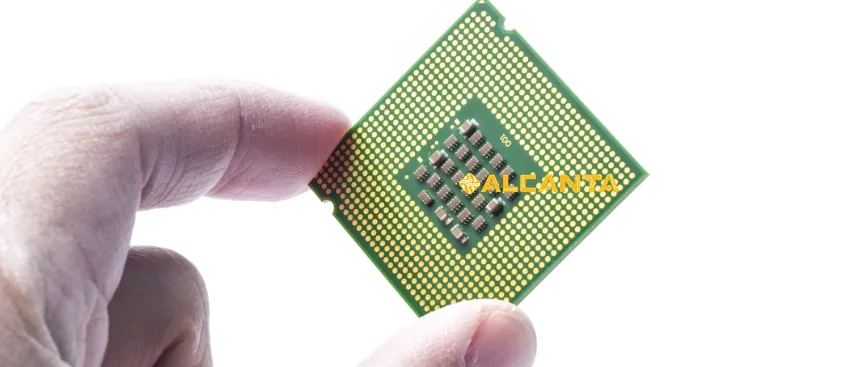
Unveiling Precision: Etch Back’s Role in BGA Substrate Quality
Etch back, a pivotal process in semiconductor manufacturing, involves selectively removing material from the surface of a substrate to enhance its properties. In the realm of Ball Grid Array (BGA) substrate production, etch back plays a paramount role. It ensures the precise modification of substrate layers, optimizing electrical performance and thermal conductivity. By meticulously controlling material removal, etch back refines the substrate’s surface, paving the way for seamless integration of semiconductor components. This process is indispensable in achieving the stringent specifications demanded by modern electronic devices. In the following discourse, we delve into the intricacies of etch back, unraveling its nuances and its profound impact on the evolution of BGA substrate technology.
Understanding Etch Back
Exploring the Etch Back Process:
Etch back is a precision manufacturing technique utilized in semiconductor fabrication to selectively remove material from the surface of a substrate. This process typically involves the use of chemical etchants or plasma to achieve controlled material removal. The substrate undergoes a series of steps including masking, etching, and cleaning to achieve the desired surface modification.
Different Techniques: Plasma Etchback vs. PCB Etchback:
Plasma etchback and PCB etchback are two primary techniques employed in semiconductor manufacturing for etch back processes.
1. Plasma Etchback: Plasma etchback utilizes a high-energy plasma to remove material from the substrate surface. This technique offers exceptional precision and control over material removal, making it suitable for applications requiring fine-tuned surface modifications. Plasma etchback is often favored for its ability to achieve uniform etching across large substrate areas.
2. PCB Etchback: PCB etchback, on the other hand, involves the use of chemical etchants to selectively remove material from the substrate surface. This technique is commonly used in printed circuit board (PCB) manufacturing, where precise control over material removal is crucial for achieving desired circuitry patterns and interconnects.
Role of Etch Back in Shinko Substrate Enhancement:
In the realm of Shinko substrate manufacturing, etch back plays a critical role in enhancing substrate performance and reliability. By selectively removing material from the substrate surface, etch back improves surface smoothness, eliminates defects, and enhances layer uniformity. These improvements contribute to the overall quality and functionality of Shinko substrates, making them ideal for high-performance applications in various industries including telecommunications, automotive, and consumer electronics. Etch back ensures that Shinko substrates meet the stringent requirements of modern electronic devices, offering superior electrical performance, thermal conductivity, and reliability.
Positive vs. Negative Etchback
Positive Etchback: Enhancing Surface Smoothness
Positive etchback is a process aimed at improving the surface smoothness of a substrate by selectively removing material from its surface. This technique involves controlled material removal to eliminate surface roughness, irregularities, and defects. By smoothing out the substrate surface, positive etchback enhances the overall quality and reliability of the substrate, making it suitable for high-performance applications. The process is particularly beneficial for achieving precise interconnections and fine-pitch features in semiconductor devices. Positive etchback ensures that the substrate’s surface meets the stringent requirements of modern electronic packaging, facilitating seamless integration and improved electrical performance.
Negative Etchback: Improving Layer Uniformity
In contrast, negative etchback focuses on improving the uniformity of substrate layers by selectively removing material from specific regions. This technique is commonly employed to address variations in layer thickness and composition across the substrate surface. Negative etchback allows for the controlled removal of excess material, thereby achieving a more uniform substrate structure. By improving layer uniformity, negative etchback enhances the substrate’s electrical properties, thermal conductivity, and mechanical stability. This process is crucial for ensuring consistent performance and reliability of semiconductor devices, especially in complex electronic systems where uniformity is paramount. Negative etchback plays a vital role in optimizing substrate manufacturing processes and enhancing the overall quality of electronic components.
Benefits of Etch Back in BGA Substrate
Enhanced Electrical Performance:
Etch back processes in BGA substrate manufacturing contribute significantly to enhanced electrical performance. By precisely controlling material removal from the substrate surface, etch back ensures uniformity in electrical properties across the substrate. This uniformity is crucial for minimizing signal loss, crosstalk, and impedance variations, thereby optimizing the performance of integrated circuits mounted on the substrate. Additionally, the improved surface smoothness resulting from etch back reduces parasitic capacitance and inductance, further enhancing signal integrity and transmission speed in high-frequency applications.
Improved Heat Dissipation:
In BGA substrates, efficient heat dissipation is essential for maintaining the optimal operating temperature of integrated circuits and preventing thermal-induced failures. Etch back processes play a vital role in enhancing heat dissipation by optimizing the substrate’s thermal conductivity. By removing excess material and refining the substrate’s surface, etch back reduces thermal resistance and improves heat transfer between the integrated circuits and the surrounding environment. This results in lower junction temperatures, increased thermal stability, and improved overall reliability of the electronic system, especially in high-power applications and harsh operating conditions.
Increased Reliability and Durability:
Etch back processes contribute to the increased reliability and durability of BGA substrates by improving their structural integrity and resistance to mechanical stress. The controlled removal of material during etch back eliminates surface defects, weak spots, and inconsistencies, thereby enhancing the substrate’s mechanical strength and resistance to deformation. This is particularly important for BGA substrates subjected to mechanical loading during assembly, handling, and operation. Additionally, the uniformity achieved through etch back ensures consistent electrical performance and thermal behavior across the substrate, reducing the likelihood of premature failure and enhancing the overall longevity of electronic devices and systems.
In summary, the benefits of etch back in BGA substrate manufacturing include enhanced electrical performance, improved heat dissipation, and increased reliability and durability, making it a critical process for achieving high-quality, high-performance electronic components and systems.
Applications of Etch Back BGA Substrate
High-Performance Computing (HPC):
In the realm of high-performance computing (HPC), where speed, reliability, and efficiency are paramount, etch back BGA substrates play a crucial role. These substrates provide the foundation for high-speed data processing, memory storage, and parallel computing systems. Etch back processes ensure uniformity in electrical properties and thermal conductivity, enabling the seamless integration of complex integrated circuits and interconnects. BGA substrates with optimized electrical performance and heat dissipation capabilities are well-suited for HPC applications such as supercomputers, data centers, and cloud computing infrastructure, where massive computational power and reliability are essential.
Automotive Electronics:
The automotive industry relies on advanced electronic systems for vehicle control, safety, infotainment, and connectivity. Etch back BGA substrates find extensive use in automotive electronics due to their ability to withstand harsh operating conditions, temperature fluctuations, and mechanical stress. These substrates provide a reliable platform for the integration of automotive control units, sensor modules, communication systems, and onboard computing devices. Etch back processes ensure the uniformity and reliability of electrical connections, contributing to the overall performance, durability, and safety of automotive electronic systems, including engine control units, advanced driver-assistance systems (ADAS), and in-vehicle entertainment systems.
Telecommunications:
Telecommunications infrastructure relies on high-speed data transmission, signal processing, and network connectivity to support a wide range of services and applications. Etch back BGA substrates play a critical role in telecommunications equipment, including routers, switches, base stations, and optical networking devices. These substrates enable the integration of high-density integrated circuits, RF components, and optical modules, facilitating efficient data routing, signal amplification, and modulation. Etch back processes ensure the uniformity of signal paths, impedance matching, and thermal management, enhancing the reliability, performance, and scalability of telecommunications equipment in demanding environments such as data centers, telecommunications networks, and mobile communication systems.
In summary, etch back BGA substrates find diverse applications in high-performance computing, automotive electronics, and telecommunications, where they provide the foundation for reliable, high-speed electronic systems that meet the stringent requirements of modern industries and applications.
Future Trends and Innovations
Advancements in Etch Back Technology:
The future of etch back technology is poised for significant advancements driven by ongoing research, innovation, and technological breakthroughs. One of the key areas of development is the refinement of etch back processes to achieve even greater precision, control, and efficiency. Researchers are exploring novel materials, chemicals, and plasma sources to enhance etch selectivity, uniformity, and speed. Additionally, there is a growing focus on developing in-situ monitoring and control techniques to optimize process parameters in real-time, ensuring consistent and reproducible results.
Another promising trend is the integration of advanced modeling and simulation tools to predict and optimize etch back processes at the atomic and molecular level. By leveraging computational modeling, researchers can gain deeper insights into the fundamental mechanisms governing material removal, surface interactions, and etch profile evolution. This enables the design of customized etch back processes tailored to specific substrate materials, device geometries, and performance requirements.
Furthermore, the advent of emerging technologies such as machine learning, artificial intelligence, and automation is expected to revolutionize etch back manufacturing processes. These technologies enable intelligent process control, predictive maintenance, and adaptive optimization, leading to improved productivity, yield, and cost-effectiveness.
Potential Impact on Semiconductor Industry:
The advancements in etch back technology are poised to have a profound impact on the semiconductor industry, shaping the future of device manufacturing, packaging, and integration. Enhanced etch back processes enable the fabrication of next-generation semiconductor devices with unprecedented performance, functionality, and reliability.
Improved surface smoothness, layer uniformity, and material selectivity resulting from advanced etch back techniques contribute to the development of high-density, high-speed integrated circuits for applications such as artificial intelligence, internet of things, and 5G communication.
Moreover, the increased adoption of etch back technology facilitates the development of advanced packaging solutions such as system-in-package (SiP), wafer-level packaging (WLP), and 3D integration. These packaging technologies enable the integration of multiple functions, components, and sensors into compact, cost-effective packages, addressing the growing demand for miniaturization, portability, and energy efficiency in consumer electronics, automotive, and healthcare industries.
In conclusion, the ongoing advancements in etch back technology hold great promise for driving innovation, competitiveness, and sustainability in the semiconductor industry, enabling the development of next-generation electronic devices and systems that push the boundaries of performance, functionality, and reliability.
FAQs about etch back bga substrateetch back bga substrate
Etch back plays a crucial role in BGA substrate production by improving the substrate’s surface quality, ensuring uniformity in layer thickness, and enhancing electrical performance. It contributes to the overall reliability, durability, and functionality of electronic devices mounted on the substrate.
Two primary techniques used in etch back for BGA substrates are plasma etchback and PCB etchback. Plasma etchback utilizes high-energy plasma to remove material, while PCB etchback involves chemical etchants. Both techniques are aimed at achieving controlled material removal and surface modification.
Etch back in BGA substrates offers several benefits, including enhanced electrical performance, improved heat dissipation, and increased reliability and durability. It ensures uniformity in electrical properties, reduces thermal resistance, and enhances the structural integrity of the substrate.
Etch back BGA substrates find applications in various industries, including high-performance computing (HPC), automotive electronics, and telecommunications. They are used in electronic components and systems requiring high reliability, thermal management, and electrical performance.

