
Understanding BGA Substrate Thickness Dynamics
In the intricate world of electronic packaging, Ball Grid Array (BGA) technology stands as a pivotal advancement. BGA packages have revolutionized the way electronic components are interconnected on circuit boards, offering enhanced performance, reliability, and compactness. Central to the functionality of BGA packages is the substrate, a foundational layer that hosts the intricate network of connections. Among the myriad factors influencing BGA performance, substrate thickness emerges as a critical consideration. This introductory section sets the stage for a comprehensive exploration of BGA substrate thickness, delving into its significance, types, standard sizes, and distinguishing features compared to related technologies. By understanding the role of substrate thickness, we uncover key insights into optimizing BGA performance and reliability.
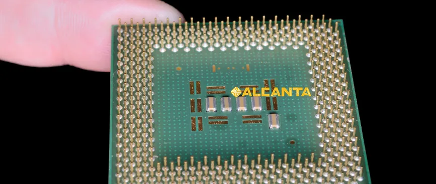
Understanding BGA Substrate
In the realm of Ball Grid Array (BGA) technology, the substrate plays a pivotal role as the foundation upon which the intricate network of connections is built. The substrate serves as the structural support for the BGA package, providing mechanical stability while facilitating electrical connections between the integrated circuit (IC) and the printed circuit board (PCB).
BGA substrates come in various types, with materials such as organic substrates being widely utilized. For instance, Kyocera organic substrates are renowned for their reliability and performance in BGA packages. These substrates are engineered to withstand the rigors of electronic applications while maintaining electrical integrity.
The choice of substrate material is crucial as it directly impacts the electrical performance of the BGA package. The substrate acts as a medium for transmitting signals between the IC and the PCB, and its properties, including dielectric constant, thermal conductivity, and coefficient of thermal expansion, significantly influence signal integrity and reliability.
Furthermore, the substrate material must possess suitable thermal properties to dissipate heat generated by the IC during operation. Efficient thermal management is essential to prevent overheating and ensure the long-term reliability of the BGA package.
In essence, the substrate in BGA technology serves as the backbone that supports electrical and mechanical functions, making it a critical component in ensuring the performance and reliability of electronic devices. Understanding the nuances of substrate materials and their impact on electrical performance is key to optimizing BGA designs for various applications.
CSP Substrate vs. TFBGA
When delving into advanced packaging technologies like Chip Scale Package (CSP) and Thin and Fine Ball Grid Array (TFBGA), understanding their substrate intricacies is essential for informed decision-making. Let’s explore the comparative aspects of these substrates:
1. Size and Thickness:
– CSP: As the name suggests, CSPs boast compact dimensions, often comparable to the size of the integrated circuit they encapsulate. This miniaturization is achieved by minimizing non-functional elements, resulting in a substrate that closely matches the IC footprint. CSP substrates typically have a thin profile to maintain the overall compactness of the package.
– TFBGA: TFBGA substrates are characterized by their fine pitch and thin profile. While they may not match the compactness of CSPs in terms of footprint, TFBGA packages excel in accommodating a high number of interconnects within a limited space. TFBGA substrates are engineered to be thin to support the fine pitch ball grid array configuration.
2. Application:
– CSP: CSPs are favored in applications where space is at a premium, such as mobile devices, wearables, and IoT (Internet of Things) devices. Their small form factor and minimal footprint make them ideal for integrating complex functionality into confined spaces.
– TFBGA: TFBGA packages find application in a wide range of electronic devices, including consumer electronics, automotive systems, and telecommunications equipment. Their ability to accommodate a high density of interconnects makes them suitable for applications requiring high-speed data processing and connectivity.
3. Electrical Performance:
– CSP: While CSP substrates are designed to be compact, they must still meet stringent electrical requirements to ensure signal integrity and reliability. Manufacturers employ advanced substrate materials and manufacturing processes to achieve optimal electrical performance while minimizing size and thickness.
– TFBGA: TFBGA substrates are engineered to support high-speed data transmission and signal integrity. The thin profile of TFBGA substrates helps mitigate signal propagation delays and impedance mismatches, contributing to enhanced electrical performance in high-frequency applications.
In summary, while both CSP and TFBGA substrates offer compact packaging solutions, they cater to different application requirements and design constraints. Understanding the nuances of their size, thickness, and electrical performance is crucial for selecting the optimal packaging solution for a given application.、
Exploring BGA Standard Sizes
1. Overview of Standard BGA Sizes:
– BGA packages come in a variety of standard sizes, ranging from small to large, to accommodate diverse application requirements.
– Common BGA sizes include 5×5 mm, 8×8 mm, 10×10 mm, and 15×15 mm, although smaller and larger sizes are also available depending on the specific needs of the application.
– The number of balls in a BGA package can vary significantly, with some packages containing just a few dozen balls to others containing several hundred or even thousands.
2. Factors Influencing BGA Size Selection:
– Application Requirements: The primary consideration when selecting a BGA size is the specific requirements of the application. Factors such as the complexity of the integrated circuit, the number of I/Os (Input/Output), and the space constraints of the PCB (Printed Circuit Board) must be taken into account.
– Signal Integrity: Larger BGA packages typically offer more space for routing traces between balls, which can help maintain signal integrity, especially in high-speed applications. However, smaller packages may be preferable in space-constrained designs despite potential signal routing challenges.
– Thermal Management: The size of the BGA package can also influence thermal management considerations. Larger packages may dissipate heat more effectively due to their larger surface area, whereas smaller packages may require additional thermal mitigation strategies.
– Manufacturing Constraints: The capabilities of the manufacturer and the assembly process can also impact BGA size selection. Some assembly processes may have limitations on the smallest or largest package sizes they can handle, as well as restrictions on ball pitch and ball diameter.
– Cost: Bigger BGA packages typically cost more due to the increased material and manufacturing complexity. Therefore, cost considerations may also play a role in determining the appropriate BGA size for a given application.
In conclusion, selecting the optimal BGA size involves balancing various factors, including application requirements, signal integrity considerations, thermal management needs, manufacturing constraints, and cost considerations. By carefully evaluating these factors, designers can choose the most suitable BGA package size to meet the unique requirements of their application while optimizing performance and cost-effectiveness.
Difference Between BGA and FBGA
1. Explanation of FBGA (Fine Ball Grid Array):
– FBGA, or Fine Ball Grid Array, represents a refinement of traditional BGA technology, specifically aimed at achieving higher pin densities and finer pitch interconnects.
– FBGA packages feature a tighter arrangement of solder balls with smaller pitches, allowing for increased I/O (Input/Output) counts within a smaller footprint.
– The advancement in manufacturing processes and materials enables the production of FBGA packages with finer features and improved electrical performance compared to conventional BGAs.
2. Distinction from Traditional BGA:
– Pitch and Density: The primary distinction between FBGA and traditional BGA lies in the pitch and density of the solder balls. FBGA packages have significantly smaller pitches, often measured in micrometers, compared to the larger pitches of conventional BGAs.
– Size and Form Factor: While traditional BGAs come in various sizes, including standard and large packages, FBGA packages are typically smaller and more compact due to the finer pitch and increased pin density.
– Application Focus: FBGA technology is often employed in high-performance and high-density applications where space constraints and signal integrity are critical, such as advanced computing systems, networking equipment, and high-speed memory modules.
– Manufacturing Precision: Manufacturing FBGA packages requires advanced fabrication techniques and precision equipment to ensure the accurate placement of solder balls with tight tolerances. This level of precision contributes to the enhanced electrical performance and reliability of FBGA packages.
3. Comparison of Substrate Thickness:
– BGA Substrate Thickness: Traditional BGA packages typically utilize substrates with moderate thickness to provide mechanical support and sufficient electrical insulation. The thickness of BGA substrates may vary depending on the specific application requirements but generally falls within a certain range to balance mechanical integrity and electrical performance.
– FBGA Substrate Thickness: In contrast, FBGA packages often incorporate thinner substrates to complement the finer pitch and smaller form factor. The reduced substrate thickness helps minimize the overall package height, enhances thermal dissipation, and improves electrical performance, especially in high-speed applications where signal integrity is paramount.
In summary, FBGA technology represents a significant evolution of traditional BGA packaging, offering higher pin densities, finer pitches, and improved electrical performance in a smaller form factor. The use of thinner substrates is one of the key differences between FBGA and traditional BGA packages, contributing to the overall advancement and miniaturization of electronic devices.
BGA vs. Micro BGA: Understanding the Contrast
1. Differentiating BGA and Micro BGA:
– Size and Pitch: The primary difference between BGA (Ball Grid Array) and Micro BGA lies in their size and pitch. While both utilize a grid of solder balls for interconnection, Micro BGA packages are significantly smaller and feature finer pitches.
– Form Factor: BGA packages come in various sizes, including standard and large configurations, whereas Micro BGA packages are specifically designed to be compact, catering to applications where space is limited.
– Application Scope: BGA packages are commonly used in a wide range of electronic devices, from consumer electronics to industrial equipment, whereas Micro BGA packages are often found in compact and portable devices such as smartphones, tablets, and wearables.
– Interconnect Density: Micro BGA packages typically boast higher interconnect densities compared to traditional BGAs, enabling the integration of complex functionality in smaller footprints.
2. Impact of Substrate Thickness on Performance and Miniaturization:
– Performance: The substrate thickness in both BGA and Micro BGA packages plays a crucial role in determining their electrical performance. Thinner substrates reduce parasitic capacitance and inductance, contributing to improved signal integrity and higher-speed operation.
– Thermal Management: Thinner substrates also enhance thermal dissipation, allowing for more efficient heat transfer from the integrated circuit to the PCB. This is particularly important in compact devices where thermal constraints are critical.
– Miniaturization: The use of thinner substrates facilitates miniaturization by reducing the overall package height. This enables designers to create slimmer and more compact electronic devices without compromising on functionality or performance.
– Manufacturing Considerations: However, thinner substrates may pose challenges during the manufacturing process, requiring precise handling and control to prevent warpage or delamination. Advanced manufacturing techniques and materials are often employed to address these challenges and ensure the reliability of Micro BGA packages.
In essence, while both BGA and Micro BGA packages offer advantages in terms of performance and miniaturization, the key differences lie in their size, pitch, and application scope. Understanding these contrasts is essential for selecting the most suitable packaging solution for a given electronic design.
FAQs about bga substrate thickness
The substrate of a BGA (Ball Grid Array) is typically composed of a material such as fiberglass epoxy resin or a ceramic material. This substrate serves as a foundation for the solder balls and provides mechanical support and electrical insulation for the integrated circuit.
The standard size of a BGA can vary depending on the specific application and manufacturer. Common BGA sizes include 5×5 mm, 8×8 mm, 10×10 mm, and 15×15 mm, though other sizes are also available. The size is chosen based on factors such as the complexity of the integrated circuit, the number of I/Os (Input/Output), and space constraints on the printed circuit board (PCB).
The primary difference between BGA (Ball Grid Array) and FBGA (Fine Ball Grid Array) lies in the pitch and density of the solder balls. FBGA packages feature smaller pitches and higher interconnect densities compared to traditional BGAs. This allows for increased I/O counts within a smaller footprint, catering to high-performance and high-density applications.
BGA (Ball Grid Array) and Micro BGA (Micro Ball Grid Array) differ primarily in size, pitch, and application scope. Micro BGA packages are significantly smaller and feature finer pitches compared to traditional BGAs. They are commonly used in compact and portable devices where space is limited, such as smartphones, tablets, and wearables, whereas traditional BGAs find application in a wider range of electronic devices.

