
Mastering BGA Substrate Routing Techniques
Ball Grid Array (BGA) technology has become pivotal in modern electronics, offering compactness and enhanced electrical performance. With its array of solder balls beneath the package, BGA facilitates high-density interconnects, enabling efficient signal transmission in complex circuitry. However, the effectiveness of BGA hinges greatly on substrate routing—the intricate process of designing pathways for electrical connections within the substrate. Substrate routing plays a crucial role in ensuring signal integrity, thermal management, and overall performance optimization of BGA packages. In this blog, we delve into the significance of BGA substrate routing and its impact on the functionality and reliability of electronic devices.
Understanding BGA Substrate
Definition of BGA Substrate:
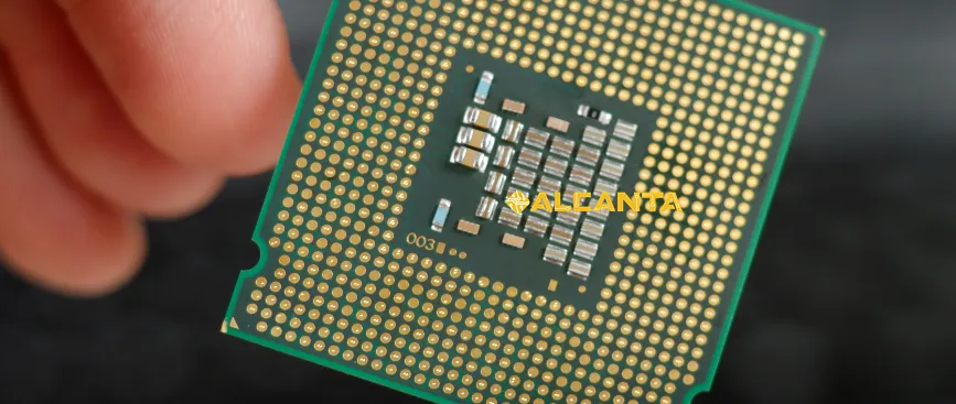
The BGA substrate is a crucial component in the packaging of integrated circuits (ICs) onto printed circuit boards (PCBs). It serves as a medium for connecting the ICs to the PCB through a dense array of solder balls or bumps arranged in a grid pattern on its underside. These solder balls establish electrical connections between the ICs and the PCB, facilitating the transmission of signals and power.
Materials Commonly Used for BGA Substrates and Their Properties:
BGA substrates are typically constructed using materials such as FR-4 (Flame Retardant 4), high-temperature laminates, ceramic, or organic substrates. FR-4 is a widely used substrate material due to its cost-effectiveness and compatibility with standard PCB manufacturing processes. High-temperature laminates offer enhanced thermal stability, making them suitable for applications requiring elevated operating temperatures. Ceramic substrates provide excellent electrical insulation and thermal conductivity, making them ideal for high-frequency and high-power applications. Organic substrates offer a balance of electrical performance, cost, and manufacturability.
Importance of Layout and Design Considerations in BGA Substrate Routing:
Effective layout and design considerations are paramount in BGA substrate routing to ensure optimal performance and reliability of electronic devices. Factors such as signal integrity, thermal management, power distribution, and manufacturability must be carefully balanced during the routing process. Proper placement of signal traces, power planes, and ground planes helps minimize signal crosstalk, impedance mismatches, and electromagnetic interference (EMI). Additionally, strategic via placement and routing techniques, such as via-in-pad or microvias, aid in optimizing signal transmission and thermal dissipation. Advanced simulation and modeling tools are often employed to validate the design and predict the behavior of BGA substrates under various operating conditions, ensuring robust performance in real-world applications.
BGA Routing Techniques
Overview of BGA Routing Methodologies:
BGA routing encompasses various techniques aimed at efficiently connecting the solder balls of the BGA package to the PCB traces. These techniques include:
– Via-in-Pad: Vias are placed directly within the pads of the BGA solder balls, allowing for shorter signal paths and improved signal integrity.
– Blind and Buried Vias: Blind vias connect an outer layer of the PCB to one or more inner layers, while buried vias connect only inner layers. These vias help in routing signals to and from the BGA package without affecting other signal layers.
– Microvias: These are small-diameter vias used to achieve higher routing density, enabling more connections in limited space. Microvias are often employed in high-density BGA designs.
Importance of Signal Integrity and Thermal Management in BGA Routing:
Signal integrity is critical in BGA routing to ensure reliable communication between the ICs and the PCB. High-speed signals traveling through BGA packages are susceptible to issues like signal degradation, reflections, and noise. Proper routing techniques, such as controlled impedance routing and differential pair routing, help mitigate these issues and maintain signal integrity.
Thermal management is equally vital to prevent overheating of BGA packages, which can lead to performance degradation and premature failure. Effective thermal vias, thermal pads, and thermal relief patterns are implemented to dissipate heat generated by the ICs and ensure optimal operating temperatures.
Techniques for Minimizing Signal Crosstalk and Impedance Mismatches in BGA Designs:
Signal crosstalk occurs when signals from adjacent traces interfere with each other, leading to signal degradation and data errors. To minimize crosstalk in BGA designs, techniques such as routing signals on different layers, increasing trace separation, and using ground planes as shields are employed.
Impedance mismatches occur when the impedance of the transmission line does not match the impedance of the connected devices, resulting in signal reflections and loss of signal quality. Techniques such as controlled impedance routing, impedance matching networks, and proper termination schemes are utilized to minimize impedance mismatches and maintain signal integrity in BGA designs. Advanced simulation tools and signal integrity analysis are often employed to validate the design and ensure compliance with performance requirements.
Key Differences: BGA vs. LGA
Comparison between Ball Grid Array (BGA) and Land Grid Array (LGA) Packaging Technologies:
BGA and LGA are both popular packaging technologies used for connecting integrated circuits (ICs) to printed circuit boards (PCBs). However, they differ significantly in their design and implementation.
– Substrate Design: In BGA packaging, solder balls are arranged in a grid pattern on the underside of the package, while in LGA packaging, metallic pads are arranged in a grid on the surface of the package. This difference in substrate design affects the routing and interconnects between the IC and the PCB.
– Soldering Methods: BGA packages are typically soldered to the PCB using reflow soldering techniques, where the solder balls are melted to create a permanent bond. In contrast, LGA packages are soldered using surface mount technology (SMT), where solder paste is applied to the PCB pads, and the package is placed on top before reflow soldering.
– Thermal Considerations: BGA packages tend to have better thermal performance compared to LGA packages due to the direct connection between the IC and the PCB, which allows for efficient heat dissipation. LGA packages may require additional thermal management solutions, such as heatsinks or thermal vias, to dissipate heat effectively.
Application Scenarios Where BGA and LGA Are Preferred:
The choice between BGA and LGA packaging depends on specific requirements and application scenarios.
– BGA Preferred Scenarios: BGA packaging is preferred in applications requiring high-density interconnects and improved thermal performance, such as mobile devices, networking equipment, and high-performance computing systems. The compact size and efficient heat dissipation of BGA packages make them suitable for space-constrained and high-temperature environments.
– LGA Preferred Scenarios: LGA packaging is favored in applications where easy reworkability and inspection are critical, such as prototyping, testing, and low-volume production. The surface-mount nature of LGA packages simplifies the soldering process and allows for easier inspection and repair compared to BGA packages. Additionally, LGA packages may be preferred in applications where the PCB layout or design constraints necessitate surface-mounted components.
BGA vs. FBGA: Unraveling the Acronyms
Differentiating between BGA (Ball Grid Array) and FBGA (Fine-Pitch Ball Grid Array) Packages:
BGA and FBGA are both types of packaging technologies used in electronic devices, but they differ in their pitch, which refers to the distance between the centers of adjacent solder balls. BGA typically has a larger pitch, while FBGA has a finer pitch, allowing for higher-density interconnects. FBGA packages often have smaller solder balls and tighter ball spacing compared to traditional BGAs.
Explaining the Evolution from Traditional BGAs to FBGAs and the Advantages They Offer:
The evolution from traditional BGAs to FBGAs has been driven by the demand for smaller, lighter, and more efficient electronic devices. As technology advances and component sizes shrink, manufacturers have developed FBGA packages to accommodate higher pin counts and finer pitch requirements. FBGAs offer several advantages over traditional BGAs, including:
– Higher pin density: FBGAs allow for more connections in a smaller footprint, enabling the integration of more functionality into compact electronic devices.
– Improved electrical performance: The finer pitch of FBGA packages reduces signal skew and crosstalk, leading to enhanced signal integrity and overall system performance.
– Enhanced thermal performance: FBGAs typically have a larger surface area for heat dissipation compared to traditional BGAs, resulting in better thermal management and reliability.
Use Cases Where FBGA Technology Excels Over Conventional BGA Packages:
FBGA technology is well-suited for applications that require high-density interconnects and improved electrical performance. Some use cases where FBGA excels include:
– High-speed communication systems: FBGA packages are ideal for high-speed interfaces such as DDR memory, PCIe, and Ethernet, where signal integrity and timing are critical.
– Mobile devices: FBGA packages allow for compact and lightweight designs, making them suitable for smartphones, tablets, and wearables.
– Networking and telecommunications equipment: FBGA technology enables the integration of complex networking functionalities into compact and efficient devices, such as routers, switches, and base stations.
In summary, FBGA technology represents the next evolution of BGA packaging, offering higher pin density, improved electrical performance, and enhanced thermal management capabilities, making it an ideal choice for a wide range of applications in the electronics industry.
Case Studies and Applications
Real-World Examples Showcasing Successful Implementations of BGA Substrate Routing:
1. Mobile Devices: In smartphones and tablets, BGA substrate routing plays a crucial role in connecting the processor, memory, and other components to the PCB. Companies like Apple and Samsung utilize advanced BGA routing techniques to achieve compact designs while ensuring high-speed data transmission and thermal management.
2. Networking Equipment: Manufacturers of networking equipment, such as Cisco and Juniper Networks, rely on BGA substrate routing for their routers, switches, and network interface cards. These devices require high-density interconnects and efficient thermal dissipation to handle large volumes of data traffic reliably.
3. Automotive Electronics: BGA substrate routing is increasingly prevalent in automotive electronics for applications such as engine control units (ECUs), infotainment systems, and advanced driver assistance systems (ADAS). Companies like Bosch and Continental leverage BGA technology to meet stringent reliability and performance requirements in harsh automotive environments.
Applications Across Various Industries:
1. Consumer Electronics: BGA substrate routing is widely used in consumer electronics products such as laptops, gaming consoles, and smart TVs. These devices benefit from the compact size, high-speed connectivity, and thermal efficiency enabled by BGA technology.
2. Automotive: In the automotive industry, BGA substrate routing is employed in vehicle ECUs, instrument clusters, navigation systems, and in-vehicle entertainment systems. The robustness and reliability of BGA packages make them suitable for automotive applications where durability and performance are paramount.
3. Telecommunications: Telecommunications equipment manufacturers rely on BGA substrate routing for networking devices, base stations, optical transceivers, and fiber optic communication systems. BGA technology enables high-speed data transmission, low latency, and efficient power management in telecommunications infrastructure.
Benefits Achieved Through Optimized BGA Routing:
– Performance: Optimized BGA routing enhances signal integrity, reduces crosstalk, and minimizes impedance mismatches, leading to improved system performance and data reliability.
– Reliability: Proper thermal management and signal integrity ensure the long-term reliability and durability of electronic devices, reducing the risk of premature failures and costly repairs.
– Cost-Efficiency: By maximizing PCB real estate and minimizing the number of layers required, optimized BGA routing can lead to cost savings in manufacturing and assembly processes. Additionally, the improved performance and reliability of BGA-enabled products contribute to lower maintenance and warranty costs over the product lifecycle.
FAQs about bga substrate routing
The substrate of a BGA (Ball Grid Array) is typically a material like FR-4 (Flame Retardant 4), high-temperature laminates, ceramic, or organic substrates. It serves as a medium for connecting integrated circuits (ICs) to printed circuit boards (PCBs) through a dense array of solder balls or bumps arranged in a grid pattern on its underside.
BGA routing involves several techniques to efficiently connect the solder balls of the BGA package to the PCB traces. Common methodologies include via-in-pad, blind and buried vias, and microvias. These techniques help optimize signal integrity, thermal management, and routing density. Additionally, careful layout and design considerations, such as signal trace placement, power distribution, and impedance matching, are essential for successful BGA routing.
The main difference between BGA (Ball Grid Array) and LGA (Land Grid Array) lies in their substrate design and soldering methods. In BGA packaging, solder balls are arranged in a grid pattern on the underside of the package, while in LGA packaging, metallic pads are arranged in a grid on the surface of the package. BGA packages are typically soldered using reflow soldering techniques, while LGA packages are soldered using surface mount technology (SMT).
The primary difference between BGA (Ball Grid Array) and FBGA (Fine-Pitch Ball Grid Array) lies in their pitch, which refers to the distance between the centers of adjacent solder balls. BGA typically has a larger pitch, while FBGA has a finer pitch, allowing for higher-density interconnects. FBGA packages often have smaller solder balls and tighter ball spacing compared to traditional BGAs.

