
Mastering the Essentials of BGA Substrate Layout
In the realm of electronics manufacturing, the Ball Grid Array (BGA) stands as a pivotal innovation, revolutionizing how components are integrated into circuit boards. Its compact design and enhanced thermal performance have made it a cornerstone in modern electronic devices, from smartphones to aerospace equipment. However, beyond its sleek appearance lies a critical aspect often overlooked—the substrate layout. In this article, we delve into the intricate world of BGA substrate layout, exploring its profound impact on circuit performance and reliability. From understanding the materials used to optimizing ball pitch and pad layout, we unravel the complexities underlying BGA assembly. Join us on a journey to uncover the hidden intricacies of BGA substrate layout and its pivotal role in shaping the future of electronics manufacturing.
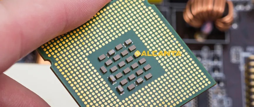
Overview of BGA Substrate
The Ball Grid Array (BGA) is a packaging technology that has transformed the landscape of electronic assemblies. At its core, the BGA comprises a silicon die encapsulated in a protective housing, with solder balls arranged in a grid pattern on the underside. This innovative structure allows for enhanced thermal dissipation and electrical performance compared to traditional packaging methods.
The working principle of BGA is straightforward yet ingenious. As electronic signals flow through the silicon die, heat is generated. The solder balls act as conduits, efficiently transferring heat away from the die to the circuit board, where it can be dissipated more effectively. This thermal management capability is especially crucial in high-performance electronic devices prone to overheating.
In modern electronic products, BGAs find widespread applications across various industries. From consumer electronics like smartphones and laptops to industrial equipment and automotive systems, BGAs are ubiquitous. Their compact size, high pin density, and reliability make them ideal for densely packed circuit boards where space is at a premium.
The advantages of BGA technology are manifold. Firstly, their compact size allows for higher component density, enabling manufacturers to design smaller and lighter devices without compromising functionality. Secondly, the solder balls provide a more reliable electrical connection, minimizing the risk of signal degradation or intermittent connections. Lastly, BGA’s superior thermal performance ensures the longevity and reliability of electronic devices, even under demanding operating conditions.
In summary, the BGA substrate represents a cornerstone in modern electronics, offering unparalleled performance, reliability, and versatility across a myriad of applications.
Significance of BGA Substrate Layout
The BGA substrate layout plays a pivotal role in determining the overall performance and stability of electronic circuits. Every aspect of the layout, from the arrangement of solder balls to the routing of traces, can significantly impact the functionality and reliability of the final product.
Emphasizing the impact of BGA substrate layout on circuit performance is crucial. The layout directly affects signal integrity, impedance matching, and thermal management. Poorly designed layouts may result in signal distortion, crosstalk, or excessive heat buildup, leading to reduced performance and potential system failures. Conversely, an optimized substrate layout ensures efficient signal transmission, minimal interference, and proper heat dissipation, thereby enhancing circuit performance and stability.
Furthermore, the importance of excellent BGA substrate layout cannot be overstated when it comes to product quality and reliability. A well-designed layout minimizes the risk of manufacturing defects such as solder bridging, open circuits, or inadequate thermal connections. This translates to higher yields during production and fewer field failures post-deployment. Moreover, a robust substrate layout contributes to the overall durability and longevity of electronic devices, ensuring they can withstand the rigors of real-world usage environments.
In essence, the BGA substrate layout serves as the foundation upon which the entire electronic system is built. By meticulously optimizing the layout to maximize performance, minimize interference, and enhance reliability, manufacturers can deliver products that meet the stringent demands of today’s technology-driven world.
Elements of BGA Substrate Layout
Substrate Material:
The choice of substrate material is a critical aspect of BGA substrate layout, influencing both performance and cost considerations. Commonly used materials include FR4, a cost-effective option with good electrical properties suitable for most applications, and high-frequency materials such as Rogers or Teflon, which offer superior signal integrity at higher frequencies but come at a higher cost.
When selecting substrate materials for BGA layouts, several factors must be considered. These include electrical properties such as dielectric constant and loss tangent, mechanical properties like thermal conductivity and coefficient of thermal expansion (CTE), as well as cost and availability. Balancing these factors ensures that the chosen material meets the specific requirements of the application while remaining within budget constraints.
Ball Pitch:
The ball pitch, or the distance between adjacent solder balls, has a significant impact on circuit layout and performance. A smaller ball pitch allows for higher pin density and more compact designs but may pose challenges in manufacturing and assembly. On the other hand, a larger ball pitch simplifies assembly but limits the number of pins and increases board size.
Determining the appropriate ball pitch involves considering various factors such as signal integrity, thermal management, and manufacturing constraints. High-speed applications may require tighter ball pitches to minimize signal distortion and impedance mismatches, while thermal considerations may dictate a larger pitch to facilitate better heat dissipation. By carefully evaluating these factors, engineers can strike a balance between performance, manufacturability, and reliability.
Pad Layout:
The layout of solder pads on the BGA substrate plays a crucial role in ensuring reliable electrical connections and optimal signal transmission. Proper pad layout follows principles such as maintaining uniform pad sizes and spacing, minimizing signal crosstalk and interference, and optimizing thermal conductivity.
Best practices for BGA pad layout include symmetric placement of pads, routing signal traces away from sensitive areas, and providing adequate thermal vias for heat dissipation. Illustrating these principles with examples demonstrates how a well-designed pad layout can enhance product performance by minimizing signal degradation, reducing electromagnetic interference (EMI), and improving thermal management.
Trace Width and Spacing:
The width and spacing of traces connecting BGA pads to other components on the circuit board are critical factors in determining signal integrity, impedance matching, and manufacturing feasibility. Wide traces reduce resistance and allow for higher current carrying capacity but may increase crosstalk and signal distortion. Narrower traces conserve board space but require careful attention to impedance control and manufacturing tolerances.
Analyzing the importance of trace width and spacing involves considering signal frequency, current requirements, and manufacturing capabilities. Methods for determining trace width and spacing include impedance calculators, simulation tools, and consultation with PCB manufacturers. By adhering to recommended guidelines and design rules, engineers can ensure optimal signal integrity and reliable operation of BGA-based electronic systems.
BGA Assembly Process
The assembly of Ball Grid Array (BGA) packages involves several intricate steps to ensure proper attachment, soldering, and inspection, ultimately guaranteeing the functionality and reliability of the electronic device.
1. Ball Attachment:
– The first step in BGA assembly involves attaching solder balls to the underside of the BGA package. This can be achieved through various methods such as solder ball placement using solder paste stencils, solder ball reflow, or the use of pre-soldered BGA packages.
2. Soldering:
– Once the solder balls are attached, the BGA package is aligned and placed onto the corresponding pads on the circuit board. The assembly is then subjected to a reflow soldering process, where heat is applied to melt the solder and create electrical connections between the BGA package and the circuit board pads.
3. Inspection:
– After soldering, the assembly undergoes thorough inspection to ensure the quality and integrity of the solder joints. This typically involves visual inspection, X-ray inspection, or automated optical inspection (AOI) to detect any defects such as solder bridges, insufficient solder, or misalignment.
Emphasis on Quality Control:
Quality control is paramount throughout the BGA assembly process to identify and rectify any defects that could compromise the performance or reliability of the electronic device.
1. Solder Paste Inspection (SPI):
– SPI is performed before BGA placement to ensure the accurate deposition of solder paste on the circuit board pads. It helps prevent issues such as insufficient or excessive solder, which can lead to poor solder joints.
2. Reflow Profile Optimization:
– Proper optimization of the reflow soldering profile is crucial to ensure consistent and reliable soldering of BGA packages. This involves fine-tuning parameters such as temperature, time, and ramp-up/down rates to achieve optimal solder joint formation without causing damage to sensitive components.
3. X-ray Inspection:
– X-ray inspection is a non-destructive testing method used to examine the internal structure of solder joints, ensuring proper alignment and solder ball integrity. It helps identify defects such as voids, cracks, or misalignments that may not be visible to the naked eye.
4. Automated Optical Inspection (AOI):
– AOI systems use cameras and image processing algorithms to detect defects in solder joints and component placement. It provides rapid and accurate inspection, allowing for quick identification and correction of assembly issues.
By implementing stringent quality control measures throughout the BGA assembly process, manufacturers can ensure the production of high-quality electronic devices that meet or exceed customer expectations for performance, reliability, and durability.
FAQs about bga substrate layout
The substrate in BGA (Ball Grid Array) is typically a thin, flat piece of material, often a laminate composed of layers of fiberglass reinforced with epoxy resin. This substrate provides a stable base for the integrated circuit (IC) chip and facilitates the connection of the solder balls to the circuit board.
The spacing for BGA pads, also known as the ball pitch, varies depending on the specific BGA package and its intended application. Common ball pitches range from around 0.5 mm to 1.0 mm, although smaller and larger pitches are also available for specialized applications.
The minimum trace width for BGA depends on factors such as the current carrying capacity, signal integrity requirements, and manufacturing capabilities. In general, trace widths for BGA routing typically range from 4 mils (0.1 mm) to 6 mils (0.15 mm) for standard applications. However, narrower traces may be used for high-density designs or high-speed signals, while wider traces may be necessary for power or ground connections.
The process of BGA assembly typically involves several steps:
Ball attachment: Solder balls are attached to the underside of the BGA package using techniques such as solder ball placement or pre-soldered BGA packages.
Placement: The BGA package is aligned and placed onto the corresponding pads on the circuit board.
Reflow soldering: The assembly undergoes a reflow soldering process, where heat is applied to melt the solder and create electrical connections between the BGA package and the circuit board pads.
Inspection: The solder joints are inspected using methods such as visual inspection, X-ray inspection, or automated optical inspection (AOI) to ensure quality and integrity.
Additional processes, such as underfill encapsulation or rework, may be performed depending on the specific requirements of the application.

