High Performance, Small Footprint: FC-CSP Substrates
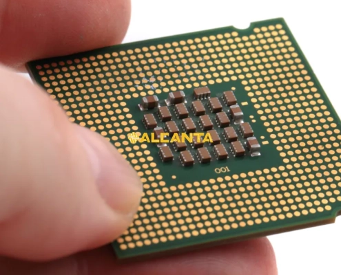
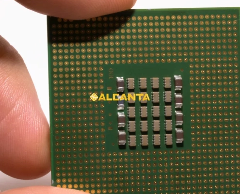
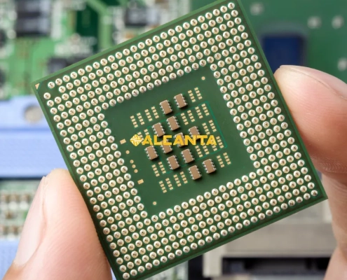
FC CSP Substrates are advanced packaging solutions that provide electrical, mechanical, and thermal connections between semiconductor chips and printed circuit boards (PCBs). These substrates use flip-chip technology, where the chip is mounted face-down, enabling shorter interconnections and improved electrical performance. They are typically made from high-density organic materials or glass, supporting fine-pitch designs and enhanced signal integrity. FC CSP Substrates are widely used in applications requiring miniaturization and high-speed processing, such as mobile devices, automotive electronics, and high-performance computing. Their compact size, excellent thermal efficiency, and electrical reliability make them essential in modern semiconductor packaging.
What Are FC CSP Substrates?
FC CSP Substrates (Flip-Chip Chip Scale Package Substrates) are essential components in semiconductor packaging, providing electrical, mechanical, and thermal connections between the chip and the printed circuit board (PCB).
Working Principle
In FC CSP packaging, the chip is mounted face-down using flip-chip technology, where solder bumps connect the chip’s electrodes directly to the substrate’s metal pads. This design shortens the signal path, improves electrical performance, increases data transmission speed, and enhances heat dissipation.
Materials and Structure
FC CSP Substrates are typically made from high-density organic materials (such as BT resin) or glass substrates, supporting fine-pitch and multi-layer routing for complex signal transmission.
Features and Advantages
- Miniaturization: Enables compact packaging for smaller electronic devices.
- High Performance: Reduces signal delay and enhances high-speed data transmission.
- Thermal Management: Improves heat dissipation for better chip reliability.
FC-CSP Substrates offer a multitude of performance advantages over traditional packaging technologies like Ball Grid Array (BGA) and Wafer Level Chip Scale Package (WLCSP). These advantages encompass various aspects such as package size, reliability, and power consumption, making FC-CSP Substrates highly desirable for a wide range of applications.
Advantages Compared to BGA and WLCSP
- Smaller Package Size: FC-CSP Substrates boast a significantly smaller footprint compared to BGA and WLCSP, enabling higher levels of miniaturization in electronic devices. This compact size is particularly advantageous in applications where space constraints are critical, such as wearable devices and portable electronics.
- Higher Reliability: The direct interconnection between the semiconductor die and the substrate in FC-CSP Substrates results in fewer solder joints and interconnects, reducing the risk of failure due to mechanical stress or thermal cycling. This enhanced reliability makes FC-CSP Substrates ideal for mission-critical applications where downtime is not an option.
- Lower Power Consumption: FC-CSP Substrates exhibit lower parasitic capacitance and resistance compared to traditional packaging technologies, resulting in reduced power consumption and improved energy efficiency. This makes them well-suited for battery-powered devices and energy-efficient electronics.
Performance in High-Frequency, High-Speed, and High-Density Applications
- 5G Communication: FC-CSP Substrates excel in high-frequency applications like 5G communication, where fast data transmission and low latency are essential. Their compact size, low parasitic capacitance, and high signal integrity make them ideal for implementing 5G modem chips and RF front-end modules.
- Artificial Intelligence: In artificial intelligence (AI) applications, where processing large volumes of data in real-time is crucial, FC-CSP Substrates offer the high-speed interconnectivity and low latency required for AI accelerators and neural network processors. Their ability to handle complex computational tasks efficiently contributes to the performance and responsiveness of AI systems.
- Internet of Things (IoT): FC-CSP Substrates play a vital role in IoT devices, enabling seamless connectivity and efficient data processing in interconnected networks. Their small form factor and low power consumption make them well-suited for IoT sensors, actuators, and edge computing devices, contributing to the scalability and reliability of IoT ecosystems.
Overall, the superior performance of FC-CSP Substrates in terms of package size, reliability, and power consumption, coupled with their exceptional capabilities in high-frequency, high-speed, and high-density applications, position them as a preferred choice for next-generation electronic devices across various industries.
FC-CSP Substrates have found widespread applications across various industries, offering unparalleled performance and reliability in demanding environments. Let’s explore some of the key application areas where FC-CSP Substrates are making significant contributions:
Smartphone Industry: In the fast-paced world of smartphones, FC-CSP Substrates play a crucial role in enabling cutting-edge features and functionalities. They are extensively used in:
- High-Definition Camera Modules: FC-CSP Substrates facilitate the integration of high-resolution image sensors, lens assemblies, and image processing chips, enabling smartphones to capture stunning photos and videos with exceptional clarity and detail.
- High-Speed Data Transmission Modules: With the increasing demand for faster data transfer rates, FC-CSP Substrates are employed in high-speed data transmission modules, enabling seamless connectivity for tasks such as video streaming, online gaming, and cloud computing on smartphones.
Automotive Electronics Sector: In the automotive industry, where safety, reliability, and performance are paramount, FC-CSP Substrates find diverse applications:
- Autonomous Driving Sensors: FC-CSP Substrates are integral components of LiDAR, radar, and camera systems used in autonomous driving technology. They enable the high-speed processing of sensor data, contributing to the accurate detection and interpretation of the vehicle’s surroundings.
- In-Car Entertainment Systems: FC-CSP Substrates power the advanced infotainment systems found in modern vehicles, providing multimedia playback, navigation, connectivity, and vehicle diagnostics features. Their compact size and high performance make them ideal for integrating multiple functions within limited space constraints.
Medical Equipment Domain: In the field of medical equipment, where precision, reliability, and portability are paramount, FC-CSP Substrates find diverse applications:
- Portable Medical Diagnostic Devices: FC-CSP Substrates enable the development of compact and lightweight diagnostic devices such as handheld ultrasound scanners, blood glucose monitors, and ECG machines. Their high performance and low power consumption make them well-suited for point-of-care testing and remote patient monitoring applications.
- Implantable Medical Devices: FC-CSP Substrates are used in implantable medical devices such as pacemakers, defibrillators, and neurostimulators. Their small form factor and biocompatible materials ensure seamless integration into the human body, providing critical therapeutic functions while minimizing discomfort to the patient.
FC-CSP Substrates play a pivotal role in advancing technological innovation and enhancing product performance across a wide range of industries, including smartphones, automotive electronics, and medical equipment. Their versatility, reliability, and high performance make them indispensable components in today’s interconnected world.
The manufacturing of FC-CSP Substrates involves a series of intricate processes and precise technologies to ensure optimal performance, reliability, and quality. Let’s explore the key manufacturing processes and the importance of quality control:
Manufacturing Processes
- Substrate Fabrication: The manufacturing process begins with substrate fabrication, where the base material, such as organic laminates or ceramics, is prepared. Advanced techniques like laser drilling and chemical etching are employed to create intricate patterns for metal layers and vias.
- Lithography: Advanced lithography techniques, including photolithography and electron beam lithography, are utilized to pattern the metal layers and create precise interconnect structures on the substrate. These techniques enable high-resolution patterning and ensure accurate alignment of components.
- Solder Mask Application: A solder mask is applied to the substrate to protect the metal traces and vias from oxidation and contamination. Precision application of solder mask materials is essential to ensure uniform coverage and optimal adhesion to the substrate.
- Soldering Processes: Precise soldering processes, such as reflow soldering or laser soldering, are employed to attach the semiconductor die to the substrate. Controlled heating and cooling cycles are crucial to achieving reliable solder joints and minimizing thermal stress on the components.
- Wire Bonding or Flip Chip Assembly: Depending on the application and design requirements, FC-CSP Substrates may undergo wire bonding or flip chip assembly processes to connect the semiconductor die to the substrate. These assembly techniques require precision alignment and bonding to ensure electrical connectivity and mechanical stability.
Quality Control
- Material Inspection: Rigorous material inspection is conducted to verify the quality and consistency of substrate materials, metal layers, solder mask materials, and solder pastes. Any deviations from specifications are identified and addressed to prevent manufacturing defects.
- Process Monitoring: Continuous monitoring of manufacturing processes, including lithography, soldering, and assembly, is essential to detect any deviations or abnormalities that may affect product quality. Real-time process control systems ensure consistency and repeatability in production.
- Functional Testing: Comprehensive functional testing is performed on finished FC-CSP Substrates to verify electrical performance, signal integrity, thermal management, and reliability under various operating conditions. This testing ensures that the substrates meet or exceed performance specifications and reliability requirements.
- Reliability Testing: FC-CSP Substrates undergo rigorous reliability testing, including temperature cycling, thermal shock, mechanical shock, and vibration testing, to simulate real-world operating conditions and identify potential failure modes. This testing validates the robustness and durability of the substrates and ensures long-term reliability in the field.
The manufacturing processes and quality control measures employed in the production of FC-CSP Substrates are critical to achieving high-performance, reliable, and cost-effective packaging solutions. By leveraging advanced technologies and stringent quality assurance practices, manufacturers can meet the demanding requirements of modern electronic devices and ensure customer satisfaction.
Future Development Trends of FC-CSP Substrates
Contact Us NOW
FAQs About FC-CSP Substrates
What is FC-CSP?
FC-CSP stands for Flip Chip Chip Scale Package. It is a type of semiconductor packaging technology that combines the advantages of Flip Chip and Chip Scale Package (CSP) techniques. FC-CSP involves directly connecting the semiconductor die to the substrate using solder bumps, eliminating the need for wire bonds. This results in a compact package with a small footprint, making it suitable for applications where space constraints are critical.
What is a semiconductor package substrate?
A semiconductor package substrate is a component of semiconductor packaging that provides a mechanical foundation for mounting and interconnecting semiconductor devices. It typically consists of a thin layer of insulating material, such as fiberglass-reinforced epoxy resin, with conductive traces patterned on its surface. The substrate serves as a platform for mounting semiconductor dies and provides electrical connections between the die and external circuitry.
What is the difference between BGA and CSP?
BGA stands for Ball Grid Array, while CSP stands for Chip Scale Package. Both are types of semiconductor packaging technologies, but they differ in their design and application:
- BGA packages feature an array of solder balls arranged in a grid pattern on the underside of the package. They typically have a larger footprint and are suitable for applications where a relatively large package size is acceptable.
- CSP packages are characterized by their compact size and minimal package-to-die size ratio. They often have no more than 1.2 times the size of the semiconductor die itself. CSP packages are ideal for space-constrained applications where miniaturization is essential.
What is embedded trace substrate?
An embedded trace substrate is a type of semiconductor package substrate where the conductive traces are embedded within the substrate material rather than being located on the surface. This design offers several advantages, including reduced signal crosstalk, improved signal integrity, and enhanced reliability. Embedded trace substrates are commonly used in high-speed and high-frequency applications where signal quality is critical, such as in telecommunications, networking, and automotive electronics.
What are FC-CSP Substrates?
FC-CSP Substrates, or Flip Chip Chip Scale Package Substrates, are advanced semiconductor packaging solutions that combine the benefits of Flip Chip and Chip Scale Package technologies. They involve directly connecting the semiconductor die to the substrate using solder bumps, resulting in a compact package with high integration and performance.
What are the key features of FC-CSP Substrates?
FC-CSP Substrates offer a compact form factor, high integration density, and enhanced electrical and thermal performance. They feature direct interconnections between the die and the substrate, reducing signal delay and enhancing signal integrity. FC-CSP Substrates are also known for their excellent thermal dissipation capabilities, making them suitable for high-power applications.
How do FC-CSP Substrates differ from traditional packaging methods like BGA?
Unlike traditional packaging methods such as Ball Grid Array (BGA), FC-CSP Substrates feature a smaller footprint and higher integration density. They eliminate the need for wire bonding, resulting in shorter interconnect lengths and improved electrical performance. FC-CSP Substrates also offer better thermal management and reliability compared to BGAs.
What are the applications of FC-CSP Substrates?
FC-CSP Substrates find applications in a wide range of industries, including consumer electronics, automotive, telecommunications, and healthcare. They are used in smartphones for high-definition camera modules and high-speed data transmission. In automotive electronics, FC-CSP Substrates are employed in autonomous driving sensors and in-car entertainment systems. Additionally, they are used in medical equipment such as portable diagnostic devices and implantable medical devices for their compact size and high reliability.


