
Exploring PCB Substrate Materials: An Essential Guide
PCB substrate materials play a pivotal role in the functionality and reliability of modern electronics. As the backbone of printed circuit boards (PCBs), these materials serve as the foundation upon which electronic components are mounted and interconnected. The transition from older wiring methods to PCBs marked a significant advancement in electronic design and manufacturing. PCBs streamlined the assembly process, reduced production costs, and enhanced the overall performance of electronic devices. This evolution revolutionized various industries, from consumer electronics to aerospace, by enabling the creation of smaller, lighter, and more complex electronic systems. Understanding the importance and characteristics of PCB substrate materials is essential for engineers and designers striving to innovate in today’s rapidly evolving electronic landscape.
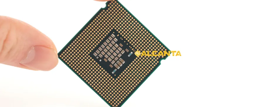
Understanding PCB Substrate Materials
Printed Circuit Board (PCB) substrates are the foundational materials upon which electronic components are mounted and interconnected to form a functional circuit. These substrates serve as the structural support for the entire electronic system and play a crucial role in determining the performance and reliability of the PCB.
Definition and Significance:
PCB substrates are typically composed of non-conductive materials, such as fiberglass-reinforced epoxy laminate (FR4), polyimide, or ceramic, which provide insulation and mechanical support for the conductive traces and components mounted on the board. The choice of substrate material significantly impacts the electrical, thermal, and mechanical properties of the PCB.
The significance of PCB substrates lies in their role as the backbone of electronic systems. They provide a platform for mounting electronic components, facilitating interconnections between them, and ensuring the structural integrity of the entire assembly. Moreover, PCB substrates enable the miniaturization of electronic devices, allowing for denser component placement and more compact designs.
Impact on PCB Performance and Reliability:
The choice of substrate material has a direct impact on the performance and reliability of the PCB. Here’s how different substrate properties influence these aspects:
1. Electrical Properties: Substrate materials affect the dielectric constant, loss tangent, and electrical impedance of the PCB. Higher-quality substrates with low dielectric loss and controlled impedance characteristics enable better signal integrity and reduce electromagnetic interference (EMI), resulting in improved overall performance.
2. Thermal Management: PCB substrates play a crucial role in dissipating heat generated by electronic components. Materials with high thermal conductivity and low thermal expansion coefficients help efficiently transfer heat away from critical components, preventing overheating and ensuring long-term reliability.
3. Mechanical Strength: The mechanical properties of the substrate, such as tensile strength, flexural strength, and dimensional stability, determine the durability and robustness of the PCB. Stiffer substrates provide better support for heavy components and prevent warping or bending during assembly and operation.
4. Chemical Resistance: PCB substrates must resist environmental factors such as moisture, chemicals, and solvents to ensure long-term reliability. Materials with good chemical resistance properties enhance the PCB’s durability and maintain performance under harsh operating conditions.
In summary, PCB substrate materials are integral to the performance, reliability, and longevity of electronic systems. Engineers must carefully select substrates based on the specific requirements of their applications to achieve optimal performance and ensure the success of their designs.
Types of PCB Substrate Materials
PCB substrate materials are available in various forms, each offering unique properties and characteristics to suit specific application requirements. Understanding the different types of substrate materials is crucial for selecting the most suitable option for a particular PCB design.
Introduction to Various Types:
1. FR4 (Fiberglass-Reinforced Epoxy Laminate): FR4 is the most widely used substrate material in PCB manufacturing. It consists of layers of woven fiberglass cloth impregnated with epoxy resin. FR4 offers excellent electrical insulation properties, mechanical strength, and dimensional stability. It is cost-effective and well-suited for a wide range of applications, from consumer electronics to industrial equipment.
Focus on FR4:
Properties: FR4 exhibits high dielectric strength, low moisture absorption, and good thermal resistance. It provides a stable platform for mounting electronic components and ensures reliable interconnections between traces.
Advantages: FR4 is readily available, cost-effective, and compatible with standard PCB manufacturing processes. It offers excellent mechanical properties, making it suitable for both rigid and flexible PCB designs.
Applications: FR4 is commonly used in electronic devices such as computers, smartphones, routers, and power supplies.
Overview of Other Substrate Materials:
2. Ceramic: Ceramic substrates are composed of materials like alumina (Al2O3) or aluminum nitride (AlN). They offer high thermal conductivity, excellent mechanical stability, and superior electrical insulation properties. Ceramic substrates are ideal for high-power applications, RF/microwave circuits, and environments requiring extreme temperature stability.
3. Polyimide: Polyimide substrates, also known as flexible PCBs, are made from heat-resistant polymer films. They offer flexibility, lightweight construction, and good chemical resistance. Polyimide substrates are commonly used in applications requiring bendability or conformal fitting, such as wearable devices, medical implants, and aerospace systems.
4. Rogers Materials: Rogers Corporation manufactures high-performance laminates specifically designed for RF/microwave applications. These materials offer low dielectric loss, controlled impedance, and excellent high-frequency performance. Rogers materials are used in RF amplifiers, antennas, radar systems, and wireless communication devices.
Conclusion:
Understanding the characteristics and properties of different PCB substrate materials is essential for designing reliable and efficient electronic systems. While FR4 remains the go-to choice for many applications due to its versatility and affordability, other materials like ceramic, polyimide, and Rogers materials offer specialized features to meet the demands of specific industries and technologies. By carefully selecting the appropriate substrate material, engineers can ensure optimal performance, reliability, and longevity of their PCB designs.
Properties of PCB Substrate Materials
PCB substrate materials exhibit a range of properties that are critical for ensuring the performance, reliability, and longevity of printed circuit boards. Understanding these properties is essential for selecting the most suitable substrate material for specific application requirements.
1. Mechanical Properties:
Tensile Strength: The ability of the substrate material to withstand stretching or pulling forces without breaking. Higher tensile strength ensures the structural integrity of the PCB during handling and operation.
Flexural Strength: The resistance of the substrate to bending or deformation under load. Substrates with high flexural strength maintain dimensional stability and prevent warping or sagging.
Dimensional Stability: The ability of the substrate to maintain its shape and dimensions under varying temperature and humidity conditions. Dimensionally stable substrates prevent changes in circuit geometry, ensuring reliable electrical connections.
2. Thermal Properties:
Thermal Conductivity: The substrate’s ability to conduct heat away from electronic components and dissipate it into the surrounding environment. Higher thermal conductivity helps prevent overheating of critical components and ensures thermal management.
Coefficient of Thermal Expansion (CTE): The rate at which the substrate expands or contracts with changes in temperature. Matching the CTE of the substrate with that of electronic components reduces the risk of mechanical stress and solder joint failure.
Thermal Resistance: The substrate’s resistance to the flow of heat through its thickness. Low thermal resistance facilitates efficient heat dissipation and improves the overall reliability of the PCB.
3. Electrical Properties:
Dielectric Constant (Dk): The ability of the substrate to store electrical energy when subjected to an electric field. Low Dk values minimize signal distortion and ensure signal integrity in high-speed digital and RF/microwave applications.
Dielectric Loss (Df): The amount of electrical energy lost as heat during signal transmission. Substrates with low dielectric loss minimize signal attenuation and maintain high-frequency performance.
Electrical Insulation: The substrate’s ability to prevent electrical leakage between conductive traces or layers. Effective electrical insulation ensures reliable isolation and prevents short circuits.
4. Chemical Properties:
Chemical Resistance: The substrate’s resistance to degradation or damage when exposed to chemicals, solvents, or environmental contaminants. Chemical-resistant substrates maintain their integrity and electrical properties in harsh operating conditions.
Moisture Absorption: The substrate’s ability to absorb moisture from the environment. Low moisture absorption reduces the risk of electrical leakage and corrosion, particularly in humid or corrosive environments.
Importance of Selecting Substrate Materials:
Selecting the appropriate substrate material based on specific application requirements is crucial for achieving optimal PCB performance and reliability. Whether it’s a high-speed digital circuit, a high-power RF amplifier, or a flexible wearable device, each application demands substrate materials with tailored mechanical, thermal, electrical, and chemical properties. By carefully considering these factors, engineers can ensure the successful design and operation of electronic systems across diverse industries and environments.
Manufacturing Process of PCB Substrates
The manufacturing process of PCB substrates involves several steps to transform raw materials into the laminates used to fabricate printed circuit boards. Here, we outline the process, focusing on FR4 as a commonly used substrate material:
1. Preparation of Raw Materials:
The manufacturing process begins with the preparation of raw materials, including fiberglass cloth, epoxy resin, and additives.
Fiberglass cloth, typically made from woven glass fibers, undergoes treatment to ensure uniformity and cleanliness.
Epoxy resin is mixed with additives such as curing agents, flame retardants, and fillers to enhance its properties and performance.
2. Impregnation of Fiberglass Cloth:
The fiberglass cloth is passed through a bath containing the epoxy resin mixture.
The cloth absorbs the resin, impregnating it thoroughly to ensure uniform distribution and saturation.
3. Layering and Lamination:
Multiple layers of impregnated fiberglass cloth are stacked together, alternating with layers of copper foil for conductor traces.
The layered stack is subjected to high temperature and pressure in a hydraulic press or lamination machine.
Heat and pressure cause the epoxy resin to cure, bonding the layers of fiberglass cloth and copper foil together to form a solid laminate.
4. Curing and Post-Treatment:
The laminated substrate undergoes a curing process, where it is heated to a specific temperature for a predetermined period.
Curing ensures complete cross-linking of the epoxy resin, resulting in a rigid and stable substrate.
Post-treatment processes such as surface treatment or coating may be applied to improve the substrate’s surface finish, adhesion properties, or solderability.
5. Mechanical Processing:
Once cured, the substrate undergoes mechanical processing steps such as drilling, routing, and profiling.
Holes are drilled through the substrate to accommodate component leads or vias for interconnection between different layers.
The substrate is cut and shaped according to the desired dimensions and specifications for the final PCB.
6. Quality Control and Testing:
Throughout the manufacturing process, quality control measures are implemented to ensure the substrate meets specifications and standards.
Testing methods such as dimensional inspection, electrical testing, and thermal analysis are performed to verify the integrity and performance of the substrate.
7. Final Inspection and Packaging:
After completion, the finished substrates undergo final inspection to check for defects or inconsistencies.
Approved substrates are packaged and prepared for shipment to PCB manufacturers, where they will be further processed to create printed circuit boards.
Conclusion:
The manufacturing process of PCB substrates, exemplified by the production of FR4 laminates, involves precise control of materials, temperature, and pressure to create high-quality substrates with consistent performance characteristics. By understanding the intricacies of substrate manufacturing, PCB designers and manufacturers can ensure the reliability and functionality of electronic systems in a wide range of applications.
Advantages of PCB Substrates
Printed Circuit Board (PCB) substrates offer numerous advantages over older wiring methods, making them the preferred choice for electronic design and manufacturing. Here, we delve into the various benefits of using PCB substrates:
1. Enhanced Reliability:
PCB substrates provide a stable and secure platform for mounting electronic components and creating interconnections.
Compared to older wiring methods such as point-to-point wiring, PCBs offer better resistance to vibration, shock, and environmental factors, ensuring long-term reliability.
2. Improved Scalability:
PCB substrates facilitate the miniaturization and densification of electronic circuits, allowing for the integration of more components in a smaller space.
With advancements in PCB fabrication techniques, designers can achieve higher component density and complexity, enabling the development of advanced electronic devices with increased functionality.
3. Cost-Effectiveness:
Although PCB fabrication involves upfront costs for design and tooling, mass production of PCBs offers economies of scale, resulting in lower per-unit costs compared to older wiring methods.
PCBs reduce labor costs associated with manual wiring and assembly, leading to overall cost savings in the manufacturing process.
4. Design Flexibility:
PCB substrates offer unparalleled design flexibility, allowing engineers to create intricate circuit layouts with precise control over trace routing and component placement.
Advanced design software enables rapid prototyping and iteration, streamlining the design process and reducing time-to-market for new products.
5. Improved Electrical Performance:
PCB substrates with controlled impedance characteristics ensure consistent signal integrity and minimize signal distortion, especially in high-speed digital and RF/microwave applications.
By eliminating the parasitic effects of long wire runs and reducing electromagnetic interference (EMI), PCBs enable higher performance and more reliable electronic systems.
6. Ease of Troubleshooting and Maintenance:
PCBs simplify troubleshooting and maintenance tasks by providing a structured layout of components and interconnections.
Visual inspection and diagnostic tools can easily identify and isolate faults or defects, reducing downtime and minimizing repair costs.
7. Environmental Friendliness:
PCB substrates are environmentally friendly compared to older wiring methods that often involve hazardous materials such as lead-based solder and PVC insulation.
Many PCB substrates are recyclable, reducing electronic waste and contributing to sustainability efforts.
In summary, PCB substrates offer a multitude of advantages over older wiring methods, including enhanced reliability, scalability, cost-effectiveness, design flexibility, improved electrical performance, ease of troubleshooting, and environmental friendliness. These benefits make PCBs the preferred choice for a wide range of electronic applications, from consumer electronics to industrial machinery and aerospace systems.
Applications of PCB Substrate Materials
PCB substrate materials find extensive use across various industries due to their versatility, reliability, and performance. Here, we explore the wide range of applications where PCB substrate materials are utilized:
1. Consumer Electronics:
PCBs are ubiquitous in consumer electronics devices such as smartphones, tablets, laptops, and TVs.
Miniaturization of components and high-density interconnects enabled by PCB substrates contribute to the sleek and compact designs of modern electronic gadgets.
Advanced PCB technologies like flexible and rigid-flex PCBs are employed in wearable devices, IoT (Internet of Things) products, and smart home appliances.
2. Automotive Industry:
PCB substrates play a critical role in automotive electronics, including engine control units (ECUs), infotainment systems, safety features, and navigation systems.
High-temperature and vibration-resistant PCB substrates are utilized to withstand the harsh operating conditions in automotive environments.
PCBs with specialized materials and designs are employed in electric vehicles (EVs) and autonomous driving systems to support advanced functionalities and connectivity.
3. Aerospace and Defense:
PCBs are integral components in aerospace and defense systems, including avionics, radar systems, communication equipment, and missile guidance systems.
Aerospace-grade PCB substrates are designed to meet stringent requirements for reliability, durability, and performance under extreme temperatures, pressure differentials, and vibration levels.
High-frequency PCB substrates with controlled impedance characteristics are used in satellite communication systems, airborne radar, and surveillance equipment.
4. Telecommunications:
PCB substrates form the backbone of telecommunications infrastructure, including base stations, routers, switches, and optical networking equipment.
High-speed digital PCBs with low-loss materials are utilized to support data transmission and networking protocols in telecommunications networks.
Advanced PCB technologies like multilayer boards and microstrip lines enable high-density interconnects and signal integrity in telecommunications equipment.
5. Industrial Automation and Robotics:
PCB substrates are essential components in industrial automation systems, robotic controllers, motion control systems, and factory automation equipment.
Ruggedized PCB substrates with high mechanical strength and thermal stability are employed in harsh industrial environments.
PCBs facilitate the integration of sensors, actuators, and control circuits, enabling precise and efficient operation of industrial machinery and robotic systems.
In summary, PCB substrate materials find widespread applications across diverse industries, including consumer electronics, automotive, aerospace, telecommunications, and industrial automation. Their versatility, reliability, and performance make them indispensable for the design and manufacture of advanced electronic systems that power modern technology and drive innovation across various sectors.
Future Trends in PCB Substrate Materials
As technology continues to evolve, the field of PCB substrate materials is witnessing several emerging trends and developments that are shaping the future of electronic design and manufacturing. Here are some key insights into the future of PCB substrate materials:
1. Advanced Material Technologies:
Ongoing advancements in materials science are leading to the development of novel substrate materials with enhanced properties and performance characteristics.
Researchers are exploring the use of nanomaterials, such as graphene and carbon nanotubes, to improve the electrical, thermal, and mechanical properties of PCB substrates.
New composite materials and hybrid structures are being developed to achieve a balance between lightweight construction, high strength, and excellent electrical conductivity.
2. High-Frequency and RF/Microwave Applications:
With the proliferation of wireless communication technologies and the Internet of Things (IoT), there is a growing demand for PCB substrates optimized for high-frequency and RF/microwave applications.
Future PCB designs will incorporate materials with ultra-low dielectric constants and loss tangents to minimize signal loss and improve signal integrity at higher frequencies.
Advancements in material processing techniques, such as laser drilling and precision etching, will enable the fabrication of PCB substrates with finer features and tighter tolerances for RF/microwave circuits.
3. Flexible and Stretchable Substrates:
The rise of wearable electronics, flexible displays, and bendable devices is driving the development of flexible and stretchable PCB substrates.
Future PCB designs will leverage materials such as polyimide, elastomers, and flexible polymers to create substrates that can conform to irregular shapes and withstand bending and stretching without compromising performance.
Stretchable PCB substrates will enable innovative applications in healthcare, fitness tracking, and human-machine interfaces, where flexibility and comfort are essential.
4. Sustainable and Environmentally Friendly Materials:
As environmental concerns become increasingly prominent, there is a growing focus on developing sustainable and environmentally friendly PCB substrate materials.
Researchers are exploring bio-based materials, recyclable polymers, and eco-friendly manufacturing processes to reduce the environmental footprint of PCB production.
Future PCB designs will prioritize materials that are non-toxic, biodegradable, and energy-efficient, aligning with the principles of circular economy and sustainable development.
5. Integration of Advanced Technologies:
PCB substrate materials will play a crucial role in the integration of advanced technologies such as 5G, artificial intelligence (AI), and quantum computing.
Future PCB designs will require substrates with superior thermal management capabilities to dissipate heat generated by high-power components and processors.
Multifunctional substrates with embedded sensors, energy harvesting capabilities, and self-healing properties will enable the development of intelligent and autonomous electronic systems.
In conclusion, the future of PCB substrate materials is characterized by ongoing innovation and advancements driven by materials science, technology trends, and evolving industry demands. By embracing emerging technologies and materials, PCB designers and manufacturers can unlock new possibilities for creating next-generation electronic devices with improved performance, reliability, and sustainability.
FAQs about 3d chip packaging
PCB substrate is typically made of a non-conductive material, such as fiberglass-reinforced epoxy laminate (FR4), polyimide, ceramic, or Rogers materials. These substrates provide structural support and insulation for the conductive traces and components mounted on the PCB.
The substrate layer of a PCB board refers to the base material on which the conductive traces and components are mounted. It serves as the foundation of the PCB and provides mechanical support and insulation. The substrate layer is usually made of materials like FR4, polyimide, or ceramic.
The base material of a PCB refers to the substrate layer on which the conductive traces and components are deposited or attached. It forms the core structural element of the PCB and determines its mechanical, thermal, and electrical properties. Common base materials include FR4, polyimide, and ceramic.
Fiberglass PCB substrate material, also known as fiberglass-reinforced epoxy laminate (FR4), is a type of substrate material widely used in PCB manufacturing. It consists of layers of woven fiberglass cloth impregnated with epoxy resin. FR4 offers excellent electrical insulation, mechanical strength, and dimensional stability, making it suitable for a wide range of electronic applications. It is one of the most common and cost-effective substrate materials used in PCB fabrication.

