
QFN Packaging: Compact Design, Robust Performance
QFN (Quad Flat No-Lead) packaging is a type of surface-mount integrated circuit package characterized by a flat bottom surface with no leads extending from the body. Its design enables direct soldering onto the PCB, reducing the footprint and enhancing thermal and electrical performance. Originally introduced in the late 1990s, QFN packages have gained widespread adoption across various electronic devices, including smartphones, computers, and automotive electronics, due to their compact size, improved heat dissipation, and excellent electrical properties. This packaging format facilitates higher component density on PCBs, contributing to miniaturization and improved functionality in modern electronic designs.
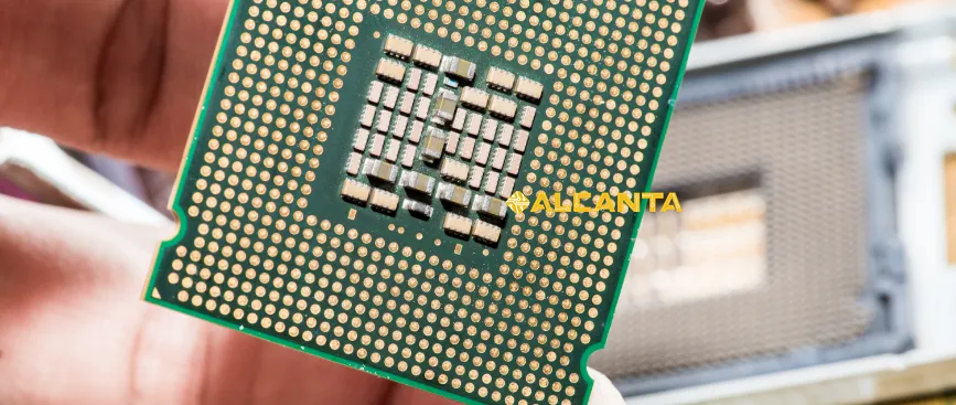
Understanding QFN Packaging
Description of QFN Package Structure and Design:
QFN packages feature a flat, square or rectangular body with exposed metal pads on the bottom surface, used for electrical connections to the PCB. Unlike traditional leaded packages, QFNs have no leads protruding from the sides, allowing for a more compact footprint. The semiconductor die is typically attached to a metal heat slug inside the package, enhancing thermal dissipation. Variations in pad configurations and sizes accommodate different pin counts and applications.
Comparison with Other Packaging Types:
– BGA (Ball Grid Array): Unlike QFN, which has exposed metal pads, BGAs use solder balls arranged in a grid on the bottom surface for connections. BGAs offer high pin counts and excellent electrical performance, but they are typically larger and more costly to manufacture than QFNs.
– QFP (Quad Flat Package): QFPs have leads extending from all four sides of the package, providing more accessibility for soldering and inspection compared to QFNs. However, QFPs generally occupy more board space and offer lower thermal dissipation capabilities.
Key Characteristics and Specifications of QFN Packages:
– Size and Footprint: QFN packages come in various sizes, ranging from small to large, catering to different pin counts and application requirements. Their compact footprint contributes to space-saving on PCBs.
– Thermal Performance: The exposed metal pad on the bottom surface of QFN packages enhances thermal conductivity, allowing for efficient heat dissipation from the semiconductor die to the PCB.
– Electrical Performance: QFN packages offer excellent electrical properties, including low parasitic inductance and capacitance, leading to improved signal integrity and high-speed performance.
– Assembly and Reliability: QFN packages are suitable for automated assembly processes such as pick-and-place and reflow soldering. Their robust design and direct PCB mounting contribute to reliable performance in various environmental conditions.
Understanding the structure, design, and specifications of QFN packages is crucial for designing and implementing electronic devices with optimal performance and reliability.
Difference between BGA and QFN
Comparison of Ball Grid Array (BGA) and QFN Packages:
BGA (Ball Grid Array):
– Structure: BGAs feature a grid of solder balls on the bottom surface, providing electrical connections to the PCB.
– Advantages: BGAs offer high pin counts, excellent electrical performance, and enhanced reliability due to the solder balls’ uniform distribution and support for fine-pitch connections.
– Disadvantages: They typically require more complex manufacturing processes and equipment due to the need for precise alignment and soldering of the solder balls. BGAs are also larger and more expensive than QFNs.
QFN (Quad Flat No-Lead):
– Structure: QFNs have a flat bottom surface with exposed metal pads for direct soldering to the PCB, eliminating the need for leads.
– Advantages: QFNs feature a compact footprint, excellent thermal dissipation, and lower manufacturing costs compared to BGAs. They also offer good electrical performance and are suitable for high-density applications.
– Disadvantages: QFNs may pose challenges in inspection and rework due to their bottom-mounted design. They also have limitations in terms of pin count compared to BGAs.
Applications and Suitability for Different Electronic Devices:
BGA:
– High-Performance Computing: BGAs are commonly used in high-performance computing devices such as CPUs, GPUs, and FPGA chips due to their high pin count and excellent electrical properties.
– Consumer Electronics: They are also found in consumer electronics like smartphones, tablets, and gaming consoles, where space-saving and high-density packaging are crucial.
QFN:
– Consumer Electronics: QFN packages are extensively used in consumer electronics for components such as microcontrollers, power management ICs, and radio frequency (RF) chips due to their compact size and good thermal performance.
– Automotive Electronics: They are also prevalent in automotive electronics for applications like engine control units (ECUs), sensors, and LED lighting due to their reliability and cost-effectiveness.
Understanding the differences between BGA and QFN packages helps designers choose the most suitable packaging solution for their electronic devices based on factors such as performance requirements, space constraints, and manufacturing considerations.
Advantages of QFN Packaging
Highlighting the Benefits of QFN Packages in Electronics Manufacturing:
1. Space-Saving Design: QFN packages offer a compact footprint due to their flat bottom surface and absence of leads, allowing for higher component density on PCBs. This space-saving design is crucial for modern electronic devices where miniaturization is essential.
2. Thermal Performance: QFNs excel in thermal management due to their direct PCB mounting and exposed metal pad on the bottom surface. This design facilitates efficient heat dissipation from the semiconductor die to the PCB, reducing the risk of overheating and improving overall system reliability.
3. Electrical Performance: QFN packages demonstrate excellent electrical properties, including low parasitic inductance and capacitance. This translates to improved signal integrity and high-speed performance, making them suitable for a wide range of electronic applications, including high-frequency and high-power applications.
Emphasis on Space-Saving Design, Thermal Performance, and Electrical Performance:
– Space-Saving Design: The compact size of QFN packages allows for more efficient use of PCB real estate, enabling the design of smaller and lighter electronic devices without compromising functionality.
– Thermal Performance: QFNs’ superior thermal conductivity helps dissipate heat generated by the semiconductor die, ensuring stable operation even under demanding conditions. This feature is particularly beneficial for power electronics and devices operating in harsh environments.
– Electrical Performance: QFN packages exhibit minimal parasitic effects, ensuring reliable signal transmission and reduced electromagnetic interference. This makes them suitable for high-speed data processing, wireless communication, and other applications requiring precise signal integrity.
Case Studies or Examples Showcasing Successful Implementation of QFN Packages:
– Mobile Devices: Many smartphones and tablets utilize QFN packages for components such as power management ICs, microcontrollers, and RF transceivers. The compact size and excellent thermal performance of QFNs contribute to the sleek design and efficient operation of these devices.
– Automotive Electronics: QFN packages are widely used in automotive electronics for applications such as engine control units (ECUs), sensors, and LED lighting modules. Their robust construction and thermal reliability ensure consistent performance in challenging automotive environments.
– Industrial Applications: In industrial settings, QFN packages are employed in control systems, motor drivers, and sensing devices where space constraints and thermal management are critical. Their combination of compact size, thermal efficiency, and electrical performance makes them ideal for demanding industrial applications.
These examples demonstrate the versatility and effectiveness of QFN packages across various industries, highlighting their role in advancing electronics manufacturing and enabling innovative product designs.
Disadvantages and Challenges of QFN Package
Identification of Potential Drawbacks and Limitations:
1. Bottom-Mounted Design: The bottom-mounted design of QFN packages can pose challenges during assembly and rework processes. Since the electrical connections are located underneath the package, visual inspection and repair become more difficult compared to packages with leads on the sides.
2. Solder Joint Reliability: QFN packages rely on solder joints between the exposed metal pads and the PCB for electrical connections. Poor soldering or inadequate soldering process control can lead to solder joint defects such as voids, cracks, or incomplete wetting, compromising the reliability of the package.
3. Thermal Cycling Stress: During operation, QFN packages may experience thermal cycling stress due to temperature variations. This can cause fatigue and eventually lead to solder joint failure, especially in applications with frequent temperature fluctuations or thermal cycling.
Discussion on Challenges in Assembly, Inspection, and Reliability:
1. Assembly Challenges: QFN packages require precise alignment during the assembly process to ensure proper soldering of the exposed metal pads to the PCB. Inadequate alignment or solder paste deposition can result in solder bridging or misalignment, affecting the electrical connections and reliability of the package.
2. Inspection Difficulties: Visual inspection of QFN packages is challenging due to their bottom-mounted design. Traditional optical inspection methods may not provide sufficient visibility of the solder joints, necessitating the use of alternative inspection techniques such as X-ray or automated optical inspection (AOI) systems.
3. Reliability Concerns: QFN packages are susceptible to reliability issues such as solder joint fatigue, delamination, and thermal mismatch between the package and the PCB. These reliability concerns become more pronounced in applications with harsh operating conditions or high-stress environments.
Strategies for Mitigating Disadvantages and Optimizing Performance:
1. Improved Soldering Process: Implementing robust soldering processes with precise control over solder paste deposition, reflow profiles, and inspection criteria can enhance solder joint reliability and minimize defects.
2. Advanced Inspection Techniques: Utilizing advanced inspection techniques such as X-ray inspection or AOI systems allows for thorough inspection of solder joints and early detection of defects, improving overall product quality and reliability.
3. Enhanced Package Design: Incorporating design features such as thermal vias, underfill encapsulation, and pad metallization enhancements can enhance the thermal performance and reliability of QFN packages, mitigating the effects of thermal cycling stress and improving long-term reliability.
By addressing these challenges through improved assembly processes, advanced inspection techniques, and enhanced package design, manufacturers can optimize the performance and reliability of QFN packages, ensuring their successful integration into electronic systems.
Difference between QFN and QFP Packages
Differentiating Quad Flat No-Lead (QFN) and Quad Flat Package (QFP) Packages:
QFN (Quad Flat No-Lead) Packages:
– Design: QFN packages feature a flat bottom surface with exposed metal pads for direct soldering to the PCB, eliminating the need for leads.
– Size: QFN packages are typically smaller and have a lower profile compared to QFP packages, making them suitable for space-constrained applications.
– Pin Configuration: QFN packages have a perimeter array of metal pads on the bottom surface, while the top surface may contain a semiconductor die or other components.
– Application Scenarios: QFN packages are commonly used in applications requiring high component density, excellent thermal dissipation, and good electrical performance.
QFP (Quad Flat Package) Packages:
– Design: QFP packages feature leads extending from all four sides of the package, providing more accessibility for soldering and inspection compared to QFN packages.
– Size: QFP packages are generally larger and have a taller profile compared to QFN packages, making them suitable for applications where space constraints are less critical.
– Pin Configuration: QFP packages have leads arranged in a grid pattern on all four sides of the package, providing more options for routing signals and power connections.
– Application Scenarios: QFP packages are suitable for applications requiring moderate component density, ease of soldering, and versatility in signal routing.
Comparison of Design, Size, Pin Configuration, and Application Scenarios:
– Design: QFN packages have a bottom-mounted design with exposed metal pads, while QFP packages have leads extending from all four sides.
– Size: QFN packages are generally smaller and have a lower profile compared to QFP packages, allowing for higher component density on the PCB.
– Pin Configuration: QFN packages typically have a perimeter array of metal pads on the bottom surface, while QFP packages have leads arranged in a grid pattern on all four sides.
– Application Scenarios: QFN packages are preferred for applications requiring compact size, high component density, and good thermal dissipation, while QFP packages are suitable for applications where ease of soldering and signal routing versatility are important.
Illustrative Examples of When to Choose QFN over QFP and Vice Versa:
– Choose QFN Over QFP:
– When designing compact and lightweight electronic devices such as smartphones, tablets, and wearables.
– When high component density and excellent thermal dissipation are required, such as in power electronics and RF applications.
– Choose QFP Over QFN:
– When ease of soldering and inspection is a priority, especially for prototypes or low-volume production.
– When signal routing flexibility is needed, allowing for easier PCB layout and design iterations in development stages.
Understanding the differences between QFN and QFP packages enables designers to select the most suitable packaging option based on the specific requirements of their electronic applications.
FAQs about qfn package datasheet
QFN packaging, or Quad Flat No-Lead packaging, is a type of surface-mount integrated circuit package characterized by a flat bottom surface with exposed metal pads used for electrical connections to the PCB. QFN packages eliminate traditional leads, allowing for a more compact footprint and improved thermal and electrical performance.
The main difference between BGA (Ball Grid Array) and QFN (Quad Flat No-Lead) packages lies in their structure and method of electrical connections. BGA packages feature a grid of solder balls on the bottom surface, providing electrical connections to the PCB, whereas QFN packages have exposed metal pads on the bottom surface for direct soldering to the PCB. Additionally, BGAs typically have higher pin counts and better electrical performance but are larger and more costly to manufacture compared to QFNs.
Some disadvantages of QFN packages include:
Difficulty in inspection and rework due to the bottom-mounted design, which makes visual inspection challenging.
Potential reliability issues related to solder joint quality and thermal cycling stress, leading to solder joint fatigue and failure over time.
Challenges in assembly, particularly precise alignment during soldering processes, which can affect the electrical connections and overall reliability of the package.
The difference between QFN (Quad Flat No-Lead) and QFP (Quad Flat Package) packages lies in their design, size, pin configuration, and application scenarios. QFN packages have a flat bottom surface with exposed metal pads for direct soldering to the PCB, while QFP packages have leads extending from all four sides of the package. QFN packages are generally smaller and have a lower profile compared to QFP packages, making them suitable for space-constrained applications. Additionally, QFN packages typically have a perimeter array of metal pads on the bottom surface, while QFP packages have leads arranged in a grid pattern on all four sides.

