
Efficient Thermal Management: Open Cavity QFN Packages
Semiconductor packaging plays a crucial role in protecting integrated circuits and facilitating their integration into electronic systems. Among the various packaging options, the Quad Flat No-leads (QFN) package has gained significant traction in recent years. QFN packaging offers a compact and reliable solution for mounting integrated circuits onto printed circuit boards (PCBs). Unlike traditional leaded packages, QFN packages feature no external leads, maximizing space efficiency and enhancing electrical performance. In this blog, we delve deeper into the world of QFN packaging, exploring its types, advantages, disadvantages, and the specific innovation of the open cavity QFN package.
Understanding QFN Packaging
Definition of QFN (Quad Flat No-leads) Package:
QFN, or Quad Flat No-leads package, is a type of surface-mount semiconductor package characterized by a flat body with no leads protruding from its sides. Instead, the package has exposed metal pads on the bottom surface, allowing for direct soldering to the PCB. QFN packages typically have a square or rectangular shape and are available in various sizes to accommodate different integrated circuit (IC) sizes and pin counts.
Key Features and Advantages:
1. Space Efficiency: QFN packages offer a compact footprint due to their leadless design, maximizing PCB real estate and enabling high-density circuit integration.
2. Improved Thermal Performance: With a large exposed metal pad on the bottom surface, QFN packages facilitate efficient heat dissipation, enhancing thermal management and reliability.
3. Low Profile: QFN packages have a low profile, making them suitable for applications with height restrictions, such as portable devices and consumer electronics.
4. Enhanced Electrical Performance: The short electrical path between the IC and the PCB, coupled with reduced parasitic effects, results in improved electrical performance, including better signal integrity and lower electromagnetic interference (EMI).
5. Cost-effectiveness: QFN packages are typically less expensive than traditional leaded packages due to their simpler design and manufacturing process.
Disadvantages of QFN Packaging:
1. Limited Thermal Dissipation: While QFN packages offer improved thermal performance compared to some other surface-mount packages, they may still face thermal limitations, especially in high-power applications or environments with restricted airflow.
2. Sensitive to Moisture and Contaminants: Exposed metal pads make QFN packages susceptible to moisture ingress and contamination during handling and assembly, potentially compromising reliability.
3. Difficulty in Rework: The absence of leads makes reworking QFN packages more challenging compared to packages with external leads, requiring specialized equipment and techniques for removal and replacement.
Understanding these key features and potential drawbacks of QFN packaging is essential for designing reliable and efficient electronic systems.
Exploring Different Types of QFN
1. Traditional QFN:
Traditional QFN packages feature a solid encapsulation around the integrated circuit, with the exposed metal pads located on the bottom surface for soldering to the PCB. These packages offer the basic benefits of QFN technology, including space efficiency, improved thermal performance, and cost-effectiveness. They are commonly used in various electronic applications where compactness and reliability are paramount.
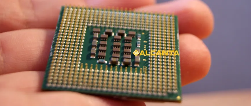
2. Open Cavity QFN:
Open cavity QFN packages, also known as cavity-down QFN, feature a cavity or recess in the center of the package, exposing the die or integrated circuit. This design allows for direct contact between the die and the PCB, enhancing thermal dissipation and electrical performance. Open cavity QFNs are particularly suitable for high-power applications where efficient heat dissipation is critical, such as power amplifiers and RF modules.
3. Air Cavity Plastic QFN:
Air cavity plastic QFN packages incorporate a hollow cavity beneath the integrated circuit, surrounded by plastic molding. This cavity reduces the overall weight of the package while providing a buffer zone for thermal expansion. Air cavity plastic QFNs offer a balance between cost-effectiveness and thermal performance, making them suitable for a wide range of consumer electronics and telecommunications applications.
4. OMPP (Over-Molded Plastic Package) QFN:
OMPP QFN packages feature a molded plastic encapsulation over the integrated circuit, similar to traditional QFNs. However, OMPP QFNs typically utilize advanced molding techniques to achieve thinner and more uniform encapsulation layers, resulting in improved thermal and electrical performance. These packages are commonly used in high-frequency and high-speed applications, such as wireless communication devices and data transmission systems.
Exploring the different types of QFN packages allows designers to select the most suitable option based on the specific requirements of their applications, balancing factors such as thermal management, electrical performance, and cost-effectiveness.
Disadvantages of QFN Packaging
1. Thermal Limitations:
QFN packages, despite their improved thermal performance compared to some other surface-mount packages, may still encounter thermal limitations, especially in high-power applications. The absence of external leads restricts the heat dissipation pathway, potentially leading to localized heating and thermal stress on the integrated circuit. In applications where significant heat generation occurs, additional thermal management techniques such as heat sinks or thermal vias may be required to mitigate thermal issues effectively.
2. Limited Flexibility in Design:
The design of QFN packages imposes certain limitations on the layout and configuration of the integrated circuit. The absence of external leads restricts the routing of signal traces and may necessitate more complex PCB layouts to accommodate the package’s footprint. Additionally, QFN packages typically have a fixed number of pins and pitch sizes, limiting the flexibility in pin count and configuration compared to packages with external leads. Designers must carefully consider these constraints when selecting QFN packages for their applications.
3. Sensitivity to Moisture and Contaminants:
QFN packages with exposed metal pads are vulnerable to moisture ingress and contamination during handling, assembly, and operation. Moisture can lead to the formation of conductive paths or corrosion on the metal surfaces, potentially causing electrical failures or reliability issues over time. Contaminants such as dust, oils, or solder flux residues can also interfere with the soldering process, affecting the quality of solder joints and overall reliability. Proper handling, storage, and assembly procedures, including moisture-sensitive packaging and cleaning processes, are essential to minimize the risk of moisture and contaminant-related failures in QFN packages.
Understanding and addressing these disadvantages of QFN packaging is crucial for mitigating potential challenges and ensuring the reliability and performance of electronic systems in which QFN packages are utilized.
Advantages of Open Cavity QFN Package
1. Enhanced Thermal Dissipation:
One of the primary advantages of open cavity QFN packages is their superior thermal dissipation capability. By exposing the integrated circuit die directly to the PCB, these packages facilitate more efficient heat transfer from the die to the surrounding environment. The absence of encapsulation material between the die and the PCB allows for better conduction and convection of heat, reducing the risk of localized hotspots and thermal stress on the IC. This enhanced thermal dissipation capability makes open cavity QFN packages particularly suitable for high-power applications where effective heat management is critical for maintaining device reliability and performance.
2. Improved Electrical Performance:
In addition to thermal benefits, open cavity QFN packages offer improved electrical performance compared to traditional QFN packages. The direct contact between the integrated circuit die and the PCB minimizes parasitic effects such as inductance and capacitance, resulting in lower signal losses and better signal integrity. The shorter electrical path between the die and external circuitry also reduces impedance and enhances high-frequency response, making open cavity QFN packages ideal for applications requiring high-speed data transmission or RF signal processing. Overall, the improved electrical performance of open cavity QFN packages contributes to enhanced system reliability and signal quality.
3. Greater Design Flexibility:
Open cavity QFN packages provide greater design flexibility compared to traditional QFN packages due to their unique construction. Designers have more freedom to optimize the layout and placement of components on the PCB, as well as the integration of thermal management features such as heat sinks or thermal vias. The exposed die also allows for direct access to the bond pads, enabling various assembly and interconnection techniques such as wire bonding or flip-chip bonding. This flexibility in design facilitates customization and optimization of electronic systems to meet specific performance requirements and space constraints, making open cavity QFN packages a versatile choice for a wide range of applications.
By leveraging these advantages, open cavity QFN packages offer a compelling solution for demanding electronic applications where efficient thermal management, superior electrical performance, and design flexibility are paramount.
Process Flow of QFN Packages
1. Substrate Preparation:
The process begins with the preparation of the substrate, typically a leadframe or a laminate-based material. The substrate is cleaned and coated with a layer of adhesive, which serves as a bonding agent for attaching the integrated circuit die.
2. Die Attach:
The next step involves die attach, where the integrated circuit die is precisely positioned and bonded to the substrate using adhesive or soldering techniques. In open cavity QFN packages, the die is placed directly onto the exposed pad on the substrate, ensuring optimal thermal and electrical contact.
3. Wire Bonding:
Once the die is attached, wire bonding is performed to establish electrical connections between the bond pads on the die and the corresponding pads on the substrate. Wire bonding can be accomplished using either gold or aluminum wire, depending on the application requirements. This step ensures proper electrical connectivity and signal transmission within the package.
4. Molding and Encapsulation:
After wire bonding, the assembly undergoes molding and encapsulation to protect the integrated circuit and wire bonds from environmental factors such as moisture, contaminants, and mechanical stresses. In this step, the assembly is encapsulated in a thermoset or thermoplastic material, which is then cured or solidified to form a protective enclosure around the die and wire bonds. For open cavity QFN packages, the encapsulation material is applied around the perimeter of the package, leaving the die and bond wires exposed.
5. Lead Finish and Singulation:
The final steps involve lead finish and singulation of the individual packages. Lead finish refers to the plating or coating applied to the exposed metal pads on the bottom surface of the package, which facilitates soldering to the PCB during assembly. Singulation involves cutting or sawing the encapsulated substrate into individual package units, ensuring proper separation between adjacent packages.
By following these sequential steps in the process flow, manufacturers can produce high-quality QFN packages with reliable electrical performance, thermal management, and environmental protection, meeting the stringent requirements of various electronic applications.
Applications of Open Cavity QFN Package
1. Aerospace and Defense:
Open cavity QFN packages find extensive use in aerospace and defense applications due to their robustness, reliability, and ability to withstand harsh environmental conditions. These packages are employed in avionics systems, radar modules, communication equipment, and navigation systems, where high performance, compact size, and resistance to shock and vibration are essential.
2. Automotive Electronics:
In the automotive industry, open cavity QFN packages are utilized in various electronic control units (ECUs), sensors, and safety systems. These packages offer excellent thermal management capabilities, making them suitable for automotive applications where temperature fluctuations and heat dissipation are significant concerns. Open cavity QFN packages are commonly found in engine control modules, airbag systems, advanced driver-assistance systems (ADAS), and infotainment systems.
3. Industrial Automation:
Open cavity QFN packages play a crucial role in industrial automation equipment and machinery, where reliability, durability, and compactness are key requirements. These packages are employed in programmable logic controllers (PLCs), motor drives, industrial sensors, and human-machine interface (HMI) devices. The enhanced thermal dissipation of open cavity QFN packages ensures reliable operation in demanding industrial environments with high temperatures, humidity, and vibration.
4. Consumer Electronics:
Open cavity QFN packages are widely used in various consumer electronics products, including smartphones, tablets, wearables, and smart home devices. These packages offer a combination of compact size, high performance, and cost-effectiveness, making them ideal for portable and handheld devices where space constraints are critical. Open cavity QFN packages can be found in applications such as wireless connectivity modules, power management ICs, audio amplifiers, and display drivers.
By catering to a diverse range of applications across different industries, open cavity QFN packages demonstrate their versatility, reliability, and effectiveness in meeting the evolving demands of modern electronic systems. Their ability to provide superior thermal dissipation, improved electrical performance, and design flexibility makes them indispensable components in a wide array of products and technologies.
FAQs about open cavity qfn package
The disadvantages of QFN (Quad Flat No-leads) packages include thermal limitations due to restricted heat dissipation pathways, limited flexibility in design due to fixed pin counts and configurations, and sensitivity to moisture and contaminants due to exposed metal pads.
QFN packaging, short for Quad Flat No-leads packaging, is a type of surface-mount semiconductor package characterized by a flat body with no external leads protruding from its sides. Instead, QFN packages feature exposed metal pads on the bottom surface for direct soldering to the PCB. They offer benefits such as space efficiency, improved thermal performance, and cost-effectiveness.
here are several types of QFN packages, including:
Traditional QFN packages, which feature solid encapsulation around the integrated circuit.
Open cavity QFN packages, with a recess exposing the die for enhanced thermal dissipation.
Air cavity plastic QFN packages, incorporating a hollow cavity for reduced weight and thermal expansion.
The process flow of QFN packages typically involves several key steps:
Substrate preparation, where the substrate is cleaned and coated with adhesive.
Die attach, where the integrated circuit die is bonded to the substrate.
Wire bonding, establishing electrical connections between the die and substrate pads.
Molding and encapsulation, protecting the assembly with a thermoset or thermoplastic material.
Lead finish, applying plating or coating to the exposed metal pads.
Singulation, cutting the substrate into individual package units.

