
The Essential Guide to Substrate Manufacturing Processe
Substrates play a crucial role in modern technology, serving as the foundational material upon which electronic components are built and interconnected. In the realm of electronics, substrates provide the mechanical support and thermal management necessary for the reliable operation of printed circuit boards (PCBs) and integrated circuits (ICs). They ensure the precise alignment of components and facilitate efficient electrical connectivity, which is essential for the performance and miniaturization of electronic devices. In the semiconductor industry, substrates are indispensable for the fabrication of microchips, where they act as the base layer for the deposition of semiconductor materials and the formation of intricate circuit patterns. Applications of substrates span across various domains, including consumer electronics, automotive systems, telecommunications, and medical devices. Their versatility and reliability make them fundamental to advancements in technology, driving innovation and enabling the development of faster, smaller, and more efficient electronic products.
What is a Substrate?
A substrate is a foundational material upon which various layers of other materials are applied, forming the base for manufacturing electronic and semiconductor components. In its simplest form, a substrate is any surface or material that acts as a support for another material or component. The term is widely used across different fields, including electronics, semiconductors, and engineering, where its properties and functions are crucial for the performance and reliability of the final products.
Definition and Basic Concept of Substrates
In electronics and semiconductor manufacturing, a substrate typically refers to the base layer of a printed circuit board (PCB) or an integrated circuit (IC). For PCBs, the substrate is usually made of insulating materials like fiberglass, epoxy, or phenolic resin, which provide structural support and electrical insulation between the conductive copper layers. In the case of ICs, the substrate is often a silicon wafer, which serves as the platform for building the complex layers of semiconductor materials that form the microelectronic circuits.
Substrates must possess several key properties to be effective, including thermal stability, electrical insulation, and mechanical strength. These properties ensure that the substrates can withstand the manufacturing processes and operational conditions without degrading or causing failure in the electronic components.
Role of Substrates in Engineering and the Semiconductor Industry
In engineering, substrates are essential for creating reliable and durable products. They provide the necessary mechanical support to electronic components, ensuring that they remain securely in place and maintain their functionality over time. Substrates also play a critical role in thermal management, helping to dissipate heat generated by electronic devices, which is crucial for preventing overheating and ensuring long-term performance.
In the semiconductor industry, substrates are fundamental to the fabrication of microchips. The silicon wafer substrates used in IC manufacturing serve as the foundation for the entire semiconductor device. These substrates must be extremely pure and free of defects to ensure the precision and efficiency of the semiconductor fabrication process. The substrate’s properties directly impact the performance of the semiconductor devices, influencing factors such as electrical conductivity, thermal management, and signal integrity.
Furthermore, substrates enable the miniaturization of electronic components, which is vital for the development of smaller, faster, and more efficient devices. As technology advances, the demand for high-performance substrates with enhanced properties continues to grow, driving innovation in substrate materials and manufacturing techniques. This ongoing development ensures that substrates remain a critical component in the advancement of modern technology.
Substrate Manufacturing Process
The manufacturing process of substrates is a complex and multi-step procedure that varies depending on the type of substrate being produced. However, the overarching goal is to create a stable, reliable base that can support and enhance the performance of electronic components. This section provides an in-depth look at the substrate manufacturing process, including the basic steps, common materials used, and the specific processes for PCB and IC substrates.
Overview of the Substrate Manufacturing Process
The substrate manufacturing process begins with the selection of raw materials and follows through a series of steps to create the final substrate. These steps ensure that the substrate meets the required mechanical, thermal, and electrical properties necessary for its intended application. The process includes material preparation, layering, and various treatments to enhance the substrate’s performance.
Basic Steps and Flow
- Material Selection: Choosing the appropriate raw materials based on the required properties of the final substrate.
- Material Preparation: Cleaning and preparing raw materials to ensure purity and eliminate contaminants.
- Layer Formation: Creating the substrate layers through processes such as lamination or deposition.
- Patterning: Defining the circuit patterns on the substrate using photolithography or other techniques.
- Etching and Plating: Removing excess material to create the desired patterns and adding metal layers to form conductive paths.
- Inspection and Testing: Conducting thorough inspections and tests to ensure the substrate meets quality standards.
Common Materials Used
The materials used in substrate manufacturing depend on the type of substrate and its intended application. Common materials include:
- Fiberglass: Used in PCB substrates for its excellent insulation and strength.
- Epoxy Resin: Provides good electrical insulation and is commonly used with fiberglass.
- Phenolic Resin: A cost-effective material used in some PCBs.
- Silicon: The primary material for IC substrates due to its semiconductor properties.
- Ceramics: Used for high-performance substrates requiring superior thermal and electrical properties.
Different Types of Substrate Manufacturing Processes
There are distinct processes for manufacturing different types of substrates, each tailored to the specific requirements of the final product.
PCB Substrate Manufacturing Process
- Lamination: Multiple layers of fiberglass and epoxy resin are laminated together under heat and pressure to form a rigid board.
- Drilling: Holes are drilled into the laminated board to allow for the insertion of through-hole components.
- Copper Plating: A thin layer of copper is plated onto the surface and through the holes to create conductive paths.
- Patterning: The copper layer is patterned using photolithography to define the circuit layout.
- Etching: Excess copper is removed through chemical etching, leaving behind the desired circuit pattern.
- Solder Mask Application: A protective solder mask is applied to prevent short circuits and protect the copper traces.
- Surface Finish: Various finishes, such as gold or silver, are applied to improve solderability and protect the copper.
IC Substrate Manufacturing Process
- Wafer Preparation: High-purity silicon ingots are sliced into thin wafers and polished to create a smooth surface.
- Oxidation: A thin layer of silicon dioxide is grown on the wafer surface to act as an insulator.
- Photolithography: Circuit patterns are transferred onto the wafer using a photomask and ultraviolet light.
- Etching: Chemical or plasma etching removes selected areas of silicon dioxide to create the desired patterns.
- Doping: Introducing impurities into specific areas of the wafer to alter its electrical properties.
- Deposition: Thin layers of materials, such as metals or dielectrics, are deposited onto the wafer to form various components of the IC.
- Planarization: The wafer surface is polished to ensure uniform thickness and smoothness.
- Packaging: The completed IC is cut from the wafer, packaged, and tested for performance.
Each of these processes is meticulously controlled to ensure the high precision and reliability required for modern electronic devices. As technology evolves, advancements in substrate materials and manufacturing techniques continue to drive the performance and capabilities of electronic components.
Substrate Manufacturing in Semiconductor
Substrate manufacturing in the semiconductor industry is a critical process that underpins the production of integrated circuits (ICs) and other microelectronic components. This section delves into the specific requirements, key materials, technologies, and detailed processes involved in the production of IC substrates, highlighting the journey from material selection to the finished product and the challenges faced along the way.
Substrate Manufacturing in the Semiconductor Industry
In the semiconductor industry, substrates serve as the foundational platform for constructing ICs. These substrates must meet stringent requirements to ensure the reliability, performance, and efficiency of the final semiconductor devices. The manufacturing process is highly specialized and involves advanced technologies to create substrates that can support the complex structures of modern ICs.
Specific Requirements and Process Needs
The manufacturing of semiconductor substrates demands high precision and strict control over various parameters to achieve the desired electrical, thermal, and mechanical properties. Key requirements include:
- High Purity: The substrates must be free of contaminants and defects to prevent interference with the semiconductor device performance.
- Thermal Stability: They should withstand high temperatures during processing and operation without degrading.
- Electrical Insulation: Substrates need to provide excellent insulation to prevent electrical shorts and ensure signal integrity.
- Mechanical Strength: Adequate mechanical strength is necessary to support the microstructures built upon them and to endure handling during manufacturing.
Key Materials and Technologies
The primary material used for IC substrates is silicon, chosen for its excellent semiconductor properties, availability, and cost-effectiveness. Other materials, such as gallium arsenide (GaAs) and silicon carbide (SiC), are used for specific applications requiring unique properties like higher electron mobility or thermal conductivity.
Key technologies involved in substrate manufacturing include:
- Crystal Growth: Methods like the Czochralski process are used to grow high-purity silicon crystals.
- Wafer Slicing: Precision slicing of silicon ingots into thin wafers.
- Chemical Vapor Deposition (CVD): Deposition of thin films of various materials onto the substrate surface.
- Photolithography: Patterning of the wafer surface to create intricate circuit designs.
- Etching: Removal of specific areas of material to define circuit elements.
Detailed Explanation of the IC Substrate Manufacturing Process
The IC substrate manufacturing process involves several detailed steps, each crucial for ensuring the quality and performance of the final product.
1. Material Selection
- Silicon Ingot Production: High-purity silicon is melted and crystallized into ingots using the Czochralski process or the float-zone technique.
- Doping: Introducing dopants to the silicon to control its electrical properties.
2. Wafer Preparation
- Slicing: Silicon ingots are sliced into thin wafers using diamond saws.
- Polishing: The wafers are polished to achieve a smooth, flat surface.
- Cleaning: Wafers are cleaned to remove any contaminants.
3. Oxidation
- Thermal Oxidation: Wafers are heated in an oxygen-rich environment to grow a thin layer of silicon dioxide on the surface, which serves as an insulating layer.
4. Photolithography
- Photoresist Application: A light-sensitive material called photoresist is applied to the wafer.
- Mask Alignment: Photomasks with the desired circuit patterns are aligned with the wafer.
- Exposure: Ultraviolet light exposes the photoresist, transferring the pattern from the mask to the wafer.
- Development: The exposed photoresist is developed, revealing the underlying silicon dioxide.
5. Etching
- Wet Etching: Chemical solutions etch away exposed areas of silicon dioxide.
- Dry Etching: Plasma etching techniques are used for more precise and controlled etching.
6. Doping
- Ion Implantation: Ions are implanted into the wafer to modify its electrical properties in specific regions.
- Annealing: Wafers are heated to repair damage from ion implantation and activate the dopants.
7. Deposition
- Chemical Vapor Deposition (CVD): Thin films of materials such as polysilicon, silicon nitride, or metals are deposited onto the wafer.
- Physical Vapor Deposition (PVD): Techniques like sputtering are used to deposit metal layers.
8. Planarization
- Chemical Mechanical Planarization (CMP): The wafer surface is polished to ensure it is flat and smooth, which is essential for subsequent layering steps.
9. Packaging
- Dicing: The wafer is cut into individual ICs.
- Mounting: ICs are mounted onto a substrate or package.
- Wire Bonding: Electrical connections are made between the IC and the package leads.
- Encapsulation: The IC is encapsulated to protect it from environmental factors.
Key Technologies and Challenges
- Miniaturization: As devices become smaller, maintaining precision in substrate manufacturing becomes more challenging.
- Material Defects: Ensuring high purity and defect-free substrates is critical, requiring advanced inspection and quality control techniques.
- Thermal Management: Efficient heat dissipation is crucial for high-performance devices, necessitating substrates with excellent thermal properties.
- Integration: Combining different materials and technologies on a single substrate to enhance functionality while maintaining performance and reliability.
The substrate manufacturing process in the semiconductor industry is a cornerstone of modern electronics, enabling the creation of powerful, efficient, and reliable devices. Continuous advancements in materials and technologies are essential to meet the growing demands of the semiconductor market.
Substrate Manufacturing Companies
Substrate manufacturing companies are vital players in the electronics and semiconductor industries, providing the essential materials and components required for a wide range of electronic devices. This section offers an overview of leading substrate manufacturing companies, including detailed company profiles, their main products and technologies, and their market positioning and impact on the industry.
Overview of Leading Substrate Manufacturing Companies
The substrate manufacturing market is dominated by a few key players who are recognized for their innovation, quality, and technological advancements. These companies are pivotal in supplying high-performance substrates for various applications, from consumer electronics to advanced semiconductor devices. Below are profiles of some of the leading companies in the substrate manufacturing industry.
Company Profiles
1. Ibiden Co., Ltd.
- Profile: Established in Japan, Ibiden is a global leader in the production of high-quality electronic components and substrates. The company has a rich history of innovation and a strong commitment to sustainability.
- Main Products and Technologies: Ibiden specializes in IC substrates, printed circuit boards (PCBs), and ceramic substrates. Their technologies include advanced multilayer substrate manufacturing and environmentally friendly production processes.
- Market Positioning and Industry Impact: Ibiden is positioned as a top-tier supplier of high-performance substrates, with a significant market share in the semiconductor and automotive industries. Their products are known for reliability and advanced performance, making them a preferred choice for leading technology companies.
2. Toppan Printing Co., Ltd.
- Profile: Toppan, also based in Japan, is a diversified printing company with a strong presence in the electronics sector. They are renowned for their cutting-edge substrate manufacturing capabilities.
- Main Products and Technologies: Toppan produces a wide range of substrates, including photomasks, IC substrates, and advanced packaging solutions. Their expertise in photolithography and fine patterning technologies is highly regarded.
- Market Positioning and Industry Impact: Toppan is a major player in the substrate market, known for its high-quality products and innovative manufacturing techniques. They are a key supplier to major semiconductor manufacturers and contribute significantly to advancements in semiconductor packaging.
3. AT&S (Austria Technologie & Systemtechnik AG)
- Profile: AT&S, headquartered in Austria, is a global leader in high-end PCB and IC substrate manufacturing. The company focuses on providing advanced solutions for the electronics industry.
- Main Products and Technologies: AT&S offers IC substrates, advanced PCBs, and high-frequency substrates. They are pioneers in using high-density interconnect (HDI) technology and embedding component technology.
- Market Positioning and Industry Impact: AT&S holds a strong market position due to their innovative solutions and high-quality products. Their substrates are used in various applications, including mobile devices, automotive electronics, and medical technology, significantly impacting the industry’s technological progression.
4. Nan Ya PCB Corporation
- Profile: Based in Taiwan, Nan Ya PCB is a leading manufacturer of PCBs and IC substrates. The company is part of the Formosa Plastics Group, one of the largest industrial conglomerates in Taiwan.
- Main Products and Technologies: Nan Ya PCB produces IC substrates, PCBs, and packaging substrates, utilizing advanced manufacturing processes such as build-up technology and surface finish technology.
- Market Positioning and Industry Impact: Nan Ya PCB is well-regarded for its high-quality products and competitive pricing. They are a significant player in the global substrate market, serving major electronics and semiconductor companies and driving innovation in substrate technology.
5. Shinko Electric Industries Co., Ltd.
- Profile: Shinko, headquartered in Japan, is a prominent manufacturer of semiconductor packages and IC substrates. The company is known for its cutting-edge technology and reliable products.
- Main Products and Technologies: Shinko specializes in flip-chip packages, multilayer substrates, and organic substrates. Their technologies include precision fabrication and advanced packaging solutions.
- Market Positioning and Industry Impact: Shinko has a strong market presence due to their technological expertise and high-performance products. They are a key supplier to major semiconductor firms and contribute to advancements in semiconductor packaging and miniaturization.
Market Positioning and Industry Impact
These leading substrate manufacturing companies play a crucial role in the electronics and semiconductor industries. Their advanced products and technologies enable the development of high-performance electronic devices, from smartphones to automotive electronics and cutting-edge semiconductor applications. The market positioning of these companies is characterized by their commitment to innovation, quality, and sustainability, which allows them to maintain strong relationships with leading technology firms and drive industry advancements.
The impact of these companies extends beyond their market share; they are instrumental in pushing the boundaries of what is possible in substrate technology. Their continuous research and development efforts lead to new materials, processes, and applications, fostering growth and innovation in the broader electronics and semiconductor sectors. As the demand for more powerful, efficient, and compact electronic devices continues to grow, the role of substrate manufacturers becomes increasingly vital, cementing their importance in the global technology landscape.
Substrate Manufacturing Examples
Substrate manufacturing encompasses a variety of processes and technologies tailored to meet the specific needs of different electronic components. This section provides detailed examples of substrate manufacturing, focusing on high-performance PCB substrates and advanced IC substrates. These examples highlight the complexities and precision involved in creating substrates that support the functionality and reliability of modern electronic devices.
Typical Examples of Substrate Manufacturing
Substrate manufacturing involves various steps and advanced technologies to produce substrates with the required properties for specific applications. Here, we explore two typical examples that illustrate the intricacies and technological advancements in substrate manufacturing.
Example 1: High-Performance PCB Substrate
High-performance printed circuit board (PCB) substrates are essential for applications that demand reliability, high-speed data transfer, and efficient thermal management. These substrates are commonly used in telecommunications, computing, and automotive electronics.
Materials and Construction:
- Base Material: High-performance PCB substrates often use materials like FR4 (a composite of fiberglass and epoxy resin) or more advanced materials like PTFE (polytetrafluoroethylene) for high-frequency applications.
- Copper Foil: A layer of copper foil is laminated onto the base material to create conductive pathways.
- Prepreg Layers: Layers of fiberglass impregnated with resin, known as prepreg, are used to bond multiple layers together.
Manufacturing Process:
- Lamination: The process begins with the lamination of multiple layers of fiberglass and resin under heat and pressure to form a rigid, multi-layered board. This creates the structural foundation of the PCB.
- Drilling: Precision drilling machines create holes for component leads and vias, which are used to connect different layers of the PCB.
- Copper Plating: The drilled holes are plated with copper to ensure electrical connectivity between layers. This step involves electroplating, where the board is submerged in a copper solution and subjected to an electric current.
- Patterning: Photolithography is used to transfer the circuit design onto the copper layer. A photoresist is applied, exposed to UV light through a mask, and then developed to reveal the desired pattern.
- Etching: The exposed copper is etched away using chemical solutions, leaving behind the circuit traces defined by the photoresist.
- Solder Mask Application: A solder mask is applied to protect the copper traces and prevent short circuits. This is typically done using a screen-printing process.
- Surface Finishing: Various finishes, such as HASL (hot air solder leveling), ENIG (electroless nickel immersion gold), or OSP (organic solderability preservative), are applied to protect the copper and enhance solderability.
- Final Testing: The finished PCB undergoes electrical testing to ensure that there are no short circuits or open circuits and that it meets the design specifications.
Applications:
- Telecommunications: Used in high-frequency communication devices like routers and switches.
- Computing: Essential for motherboards and high-speed data transfer interfaces.
- Automotive Electronics: Utilized in advanced driver-assistance systems (ADAS) and infotainment systems.
Example 2: Advanced IC Substrate
Integrated circuit (IC) substrates are crucial for the packaging and interconnection of semiconductor devices. Advanced IC substrates are used in high-performance computing, mobile devices, and other applications requiring miniaturization and high reliability.
Materials and Construction:
- Base Material: High-purity silicon wafers are commonly used, though other materials like silicon carbide (SiC) or gallium arsenide (GaAs) may be used for specific applications.
- Metal Layers: Thin layers of metals such as aluminum, copper, or gold are deposited to form electrical connections.
- Dielectrics: Materials like silicon dioxide (SiO2) or silicon nitride (Si3N4) are used as insulating layers.
Manufacturing Process:
- Wafer Preparation: High-purity silicon ingots are sliced into thin wafers and polished to create a smooth, flat surface. The wafers undergo a series of cleaning steps to remove any contaminants.
- Oxidation: The wafers are subjected to thermal oxidation to grow a thin layer of silicon dioxide on the surface, which serves as an insulating layer.
- Photolithography: Circuit patterns are transferred onto the wafer using a photomask and ultraviolet light. A photoresist is applied, exposed through the mask, and developed to reveal the circuit pattern.
- Etching: Both wet and dry etching techniques are used to remove selected areas of silicon dioxide and other materials, defining the circuit elements.
- Doping: Ions are implanted into specific areas of the wafer to modify its electrical properties. This step is followed by annealing, which heals any damage to the crystal structure and activates the dopants.
- Deposition: Thin films of conductive and insulating materials are deposited using techniques like chemical vapor deposition (CVD) and physical vapor deposition (PVD).
- Planarization: Chemical mechanical planarization (CMP) is used to ensure the wafer surface is flat and smooth, critical for building multiple layers of circuits.
- Packaging: The finished ICs are diced from the wafer, mounted onto a substrate or package, and connected using wire bonding or flip-chip technology. The ICs are then encapsulated to protect them from environmental factors.
Applications:
- High-Performance Computing: Used in CPUs, GPUs, and other high-speed processing units.
- Mobile Devices: Essential for processors and memory chips in smartphones and tablets.
- Medical Devices: Utilized in advanced diagnostic and monitoring equipment, where reliability and precision are paramount.
These examples of substrate manufacturing illustrate the intricate processes and advanced technologies involved in creating high-performance and reliable substrates for various electronic applications. The continuous innovation in materials and manufacturing techniques ensures that substrates can meet the ever-increasing demands of modern technology.
Packaging Substrate Definition
Packaging substrates play a crucial role in the realm of electronic packaging, serving as the foundational base for mounting and interconnecting semiconductor devices. Understanding what packaging substrates are and their significance in electronic packaging is essential for appreciating their contribution to the functionality and reliability of modern electronic systems.
What is a Packaging Substrate?
A packaging substrate is a material layer or structure used to support and electrically connect semiconductor devices within an electronic package. These substrates serve as the platform upon which integrated circuits (ICs) are mounted and interconnected, providing both mechanical support and electrical pathways. Packaging substrates are integral components in the assembly of electronic devices, enabling the encapsulation and protection of delicate semiconductor components while facilitating their connection to the external environment.
Definition and Role of Packaging Substrates
Definition: Packaging substrates are typically composed of materials such as organic resins, ceramics, or laminates, which offer a combination of mechanical strength, thermal conductivity, and electrical insulation. These substrates feature patterned conductive traces, vias, and pads that allow for the precise interconnection of ICs, passive components, and other electronic elements. They are used in a variety of packaging formats, including ball grid arrays (BGAs), chip-scale packages (CSPs), and flip-chip packages.
Role: The primary roles of packaging substrates include:
- Mechanical Support: Providing a stable platform for mounting semiconductor devices, ensuring physical integrity and protection from mechanical stress.
- Electrical Interconnection: Creating conductive pathways that enable the transmission of electrical signals between the ICs and the external circuitry.
- Thermal Management: Facilitating the dissipation of heat generated by the semiconductor devices to prevent overheating and ensure reliable operation.
- Protection: Shielding the ICs from environmental factors such as moisture, dust, and mechanical damage, thereby enhancing the durability and lifespan of the electronic package.
Importance in Electronic Packaging
Packaging substrates are vital to the performance and reliability of electronic devices. Their importance in electronic packaging can be highlighted through several key aspects:
1. Miniaturization: As electronic devices become increasingly compact and complex, the need for efficient and reliable packaging substrates grows. Advanced packaging substrates enable the miniaturization of electronic components by providing high-density interconnects and supporting the integration of multiple functions within a small footprint.
2. Electrical Performance: High-quality packaging substrates ensure optimal electrical performance by minimizing signal loss, reducing parasitic inductance and capacitance, and maintaining signal integrity. This is particularly crucial in high-speed and high-frequency applications, where even minor imperfections can lead to significant performance degradation.
3. Thermal Management: Effective thermal management is essential for maintaining the performance and reliability of semiconductor devices. Packaging substrates with good thermal conductivity help dissipate heat away from the ICs, preventing thermal-induced failures and ensuring stable operation.
4. Reliability and Durability: Packaging substrates enhance the reliability and durability of electronic packages by providing robust mechanical support and protection against environmental factors. This is especially important in harsh operating conditions, such as automotive, aerospace, and industrial applications.
5. Integration and Functionality: Modern packaging substrates support the integration of additional functions, such as embedded passive components, antennas, and sensors. This enables the development of more sophisticated and multifunctional electronic systems, reducing the need for discrete components and simplifying the overall design.
Example Applications:
- Mobile Devices: Packaging substrates in smartphones and tablets facilitate the integration of processors, memory, and other critical components, contributing to the devices’ compact size and high performance.
- Automotive Electronics: In automotive applications, packaging substrates support advanced driver-assistance systems (ADAS), infotainment systems, and engine control units, ensuring reliability and robustness in demanding environments.
- Medical Devices: Packaging substrates are used in medical electronics to provide reliable and durable platforms for diagnostic and monitoring devices, ensuring their performance and longevity.
Packaging substrates are indispensable components in the field of electronic packaging. Their role in providing mechanical support, electrical interconnection, thermal management, and protection is fundamental to the performance and reliability of modern electronic devices. As technology continues to advance, the development of innovative packaging substrates will remain a key driver in the evolution of electronic systems.
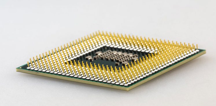
What is an IC Substrate?
Integrated Circuit (IC) substrates are fundamental components in the semiconductor industry, playing a critical role in the functionality and performance of electronic devices. This section delves into the definition and function of IC substrates and highlights the key differences between IC substrates and other types of substrates used in electronics.
Definition and Function of IC Substrates
Definition:
An IC substrate is a specialized type of substrate used to provide a base for mounting and interconnecting integrated circuits (ICs). These substrates are designed to support the ICs mechanically, electrically, and thermally, ensuring optimal performance and reliability. IC substrates are typically made from materials such as silicon, ceramic, or organic laminates, which offer a balance of mechanical strength, thermal conductivity, and electrical insulation.
Function:
The primary functions of IC substrates include:
- Mechanical Support: Providing a stable and robust platform for mounting ICs, protecting them from physical damage and ensuring their structural integrity during manufacturing, handling, and operation.
- Electrical Interconnection: Creating conductive pathways that connect the ICs to the external circuitry, enabling the transmission of electrical signals. This involves the use of fine metal traces, vias, and pads that facilitate complex interconnections.
- Thermal Management: Dissipating the heat generated by the ICs to maintain an optimal operating temperature and prevent overheating. Effective thermal management is crucial for the reliability and longevity of semiconductor devices.
- Signal Integrity: Maintaining the integrity of electrical signals by minimizing losses, interference, and cross-talk between adjacent conductive pathways. This is particularly important in high-speed and high-frequency applications.
- Integration and Miniaturization: Supporting the integration of multiple functions within a compact package, enabling the miniaturization of electronic devices. This includes the incorporation of passive components, antennas, and sensors directly into the substrate.
Differences Between IC Substrates and Other Substrates
While IC substrates share some similarities with other types of substrates used in electronics, there are key differences that distinguish them in terms of materials, construction, and applications.
1. Material Composition:
- IC Substrates: Typically made from high-purity silicon, ceramic, or advanced organic laminates. These materials are chosen for their superior electrical, thermal, and mechanical properties, which are essential for supporting high-performance semiconductor devices.
- PCB Substrates: Often made from materials like FR4 (fiberglass-reinforced epoxy laminate) or other organic composites. These materials are suitable for a wide range of applications but may not offer the same level of performance as those used in IC substrates.
2. Manufacturing Precision:
- IC Substrates: Manufactured with extremely high precision to accommodate the fine geometries and tight tolerances required for semiconductor devices. Processes such as photolithography, precision etching, and advanced deposition techniques are used to create intricate patterns and structures.
- Other Substrates: While PCB substrates also require precision, the level of detail and accuracy needed is generally lower compared to IC substrates. PCB manufacturing processes include lamination, drilling, and patterning, which are less complex than those used for IC substrates.
3. Thermal Management:
- IC Substrates: Designed to provide efficient thermal management, often incorporating materials and structures that enhance heat dissipation. This is critical for maintaining the performance and reliability of high-density semiconductor devices.
- Other Substrates: Thermal management is important but may not be as critical as in IC substrates. PCBs, for example, may use heat sinks or thermal vias to manage heat, but the overall thermal requirements are typically less demanding.
4. Application Focus:
- IC Substrates: Primarily used in semiconductor packaging, including flip-chip packages, ball grid arrays (BGAs), and chip-scale packages (CSPs). They are essential for high-performance computing, telecommunications, and advanced electronic devices.
- Other Substrates: Used in a broader range of applications, including consumer electronics, automotive electronics, and industrial systems. PCB substrates are more versatile and can be found in a wide variety of electronic products.
5. Cost and Complexity:
- IC Substrates: Generally more expensive and complex to manufacture due to the advanced materials and processes involved. The high cost is justified by the critical role they play in supporting advanced semiconductor devices.
- Other Substrates: Typically less expensive and easier to produce, making them suitable for mass-market applications where cost-efficiency is a priority.
Example Applications:
- IC Substrates: Used in microprocessors, memory chips, high-frequency RF components, and other high-performance semiconductor devices.
- PCB Substrates: Found in consumer electronics like smartphones, laptops, and televisions, as well as in automotive control systems, industrial machinery, and household appliances.
IC substrates are specialized substrates designed to meet the stringent requirements of semiconductor devices. They offer superior electrical, thermal, and mechanical properties, enabling the reliable operation of advanced electronic components. The differences between IC substrates and other types of substrates highlight the unique challenges and demands of semiconductor packaging, underscoring the critical role of IC substrates in the electronics industry.
What is the Difference Between Wafer and Substrate?
In the semiconductor industry, the terms “wafer” and “substrate” are often used, but they refer to different components with distinct roles. Understanding the definitions, uses, and main differences between wafers and substrates is essential for appreciating their functions and contributions to electronic device fabrication.
Definitions and Uses of Wafers and Substrates
Wafers
- Definition: A wafer is a thin slice of semiconductor material, typically silicon, used as the base for fabricating electronic circuits and microdevices. It serves as the foundational platform upon which integrated circuits (ICs) and other microelectronic devices are built.
- Uses: Wafers are used in the manufacturing of ICs, including microprocessors, memory chips, and sensors. They are the starting material for semiconductor device fabrication processes such as doping, etching, and deposition.
Substrates
- Definition: In a broader context, a substrate is any material that provides a surface for the construction or mounting of other materials or components. In the context of electronics, a substrate is a base material used to support electronic components, including ICs, and to provide electrical interconnections.
- Uses: Substrates are used in various applications, such as printed circuit boards (PCBs), IC packages, and other electronic assemblies. They provide mechanical support, electrical connectivity, and thermal management for electronic components.
Main Differences Between Wafers and Substrates
Materials and Structure
- Wafers: Primarily made from high-purity silicon, though other semiconductor materials like gallium arsenide (GaAs) or silicon carbide (SiC) may also be used. Wafers are single-crystal structures, providing a uniform and defect-free surface for device fabrication.
- Substrates: Can be made from a variety of materials depending on the application, including organic laminates (e.g., FR4 for PCBs), ceramics, and composite materials. Substrates often consist of multiple layers and include conductive traces and insulating layers.
Manufacturing Processes
- Wafers: The manufacturing process of wafers involves crystal growth (such as the Czochralski process), slicing the grown ingot into thin wafers, polishing, and cleaning. The wafers are then processed through various semiconductor fabrication steps, including photolithography, doping, etching, and metallization.
- Substrates: Substrate manufacturing involves creating the base material (e.g., laminating fiberglass and resin for PCBs), patterning conductive traces using photolithography or screen printing, drilling vias, and applying surface finishes. For IC substrates, additional steps like precision etching, deposition, and multi-layer lamination are involved.
Application Areas
- Wafers: Used primarily in the semiconductor industry for the fabrication of ICs and other microelectronic devices. They are essential in producing the active components of electronic systems.
- Substrates: Found in a wide range of electronic applications, including PCBs for consumer electronics, automotive control units, aerospace systems, and advanced IC packaging solutions. Substrates serve as the supporting structures for mounting and interconnecting various electronic components.
Functionality
- Wafers: Act as the platform for creating the electronic circuits and active components of microdevices. They are integral to the semiconductor manufacturing process, forming the base layer upon which all other device structures are built.
- Substrates: Provide mechanical support, electrical interconnection, and thermal management for electronic assemblies. They facilitate the integration of multiple components into a cohesive system and protect sensitive electronic parts from mechanical and environmental stress.
Example Processes
- Wafer Fabrication:
- Crystal Growth: High-purity silicon is melted and formed into a single crystal ingot using the Czochralski process.
- Slicing: The ingot is sliced into thin wafers using a diamond saw.
- Polishing: Wafers are polished to achieve a smooth, defect-free surface.
- Cleaning: Wafers undergo rigorous cleaning to remove any contaminants.
- Device Fabrication: Wafers are processed through photolithography, doping, etching, and metallization to create semiconductor devices.
- Substrate Fabrication:
- Material Preparation: Base materials such as fiberglass-reinforced resin for PCBs or ceramics for IC substrates are prepared.
- Lamination: Multiple layers of the base material are laminated together.
- Patterning: Conductive traces are patterned using photolithography or screen printing.
- Drilling: Vias are drilled to create vertical interconnections between layers.
- Finishing: Surface finishes are applied to enhance solderability and protect conductive traces.
- Assembly: Electronic components are mounted and interconnected on the substrate.
While both wafers and substrates are essential in the production of electronic devices, they serve distinct roles and are made using different materials and processes. Wafers form the basis for creating semiconductor devices, while substrates provide the supporting structure for mounting and interconnecting these devices within electronic assemblies. The differences in their materials, manufacturing processes, and applications underscore their unique contributions to the electronics industry.
What is the Difference Between PCB and Package Substrate?
Printed circuit board (PCB) substrates and package substrates are both critical components in electronic devices, but they serve distinct purposes and have unique characteristics. Understanding the differences between these two types of substrates helps in appreciating their specific roles, materials, manufacturing processes, application areas, and performance considerations.
Definitions and Uses of PCB Substrates and Package Substrates
PCB Substrates
- Definition: A PCB substrate is the foundational material upon which electronic components are mounted to form a complete circuit board. It provides mechanical support and electrical interconnections for components such as resistors, capacitors, and ICs.
- Uses: PCB substrates are used in a wide range of electronic devices, including consumer electronics (e.g., smartphones, laptops), automotive systems, industrial machinery, and household appliances. They form the backbone of most electronic assemblies, providing the structure and pathways for electrical signals.
Package Substrates
- Definition: A package substrate is a specialized type of substrate used in the packaging of integrated circuits (ICs). It serves as the base upon which the IC die is mounted and provides electrical connections between the IC and the external environment.
- Uses: Package substrates are used in semiconductor packaging formats such as ball grid arrays (BGAs), chip-scale packages (CSPs), and flip-chip packages. They are essential for high-performance computing, telecommunications, and advanced electronic devices where miniaturization and reliability are crucial.
Main Differences Between PCB Substrates and Package Substrates
Materials and Manufacturing Processes
Materials:
- PCB Substrates: Typically made from materials like FR4 (fiberglass-reinforced epoxy laminate), which offer a good balance of mechanical strength, electrical insulation, and cost-effectiveness. High-frequency PCBs may use materials such as PTFE (polytetrafluoroethylene).
- Package Substrates: Often made from materials like high-purity silicon, ceramic, or advanced organic laminates. These materials are selected for their superior thermal conductivity, electrical performance, and ability to support fine geometries.
Manufacturing Processes:
- PCB Substrates:
- Lamination: Multiple layers of fiberglass and resin are laminated together to form a rigid board.
- Drilling: Precision drilling machines create holes for vias and component leads.
- Patterning: Conductive traces are patterned using photolithography or screen printing.
- Etching: Unwanted copper is etched away to form the circuit patterns.
- Solder Mask Application: A protective solder mask is applied to prevent short circuits.
- Surface Finishing: Various finishes (e.g., HASL, ENIG) are applied to enhance solderability.
- Assembly: Electronic components are mounted and soldered onto the PCB.
- Package Substrates:
- Material Preparation: High-purity silicon or ceramic substrates are prepared.
- Patterning: Fine conductive traces are patterned using advanced photolithography.
- Via Formation: Vias are created to connect different layers and allow vertical electrical connections.
- Deposition: Thin films of metals and insulators are deposited to form interconnects.
- Encapsulation: The IC die is mounted on the substrate and encapsulated to protect it from environmental factors.
- Testing: Electrical testing is performed to ensure the functionality and reliability of the package.
Application Areas:
- PCB Substrates:
- Consumer electronics (e.g., smartphones, laptops, TVs)
- Automotive electronics (e.g., engine control units, infotainment systems)
- Industrial control systems
- Medical devices (e.g., diagnostic equipment)
- Package Substrates:
- High-performance computing (e.g., CPUs, GPUs)
- Telecommunications (e.g., RF components, base stations)
- Mobile devices (e.g., processors, memory chips)
- Aerospace and defense applications (e.g., radar systems)
Performance and Cost Comparison:
Performance:
- PCB Substrates: Designed to provide reliable performance for a wide range of applications. The performance can vary based on the materials and manufacturing processes used, with high-frequency and high-performance PCBs requiring more advanced materials and techniques.
- Package Substrates: Optimized for high-performance applications where electrical performance, thermal management, and miniaturization are critical. They support higher frequencies, greater signal integrity, and better thermal dissipation compared to typical PCB substrates.
Cost:
- PCB Substrates: Generally less expensive due to the use of cost-effective materials and simpler manufacturing processes. The cost can increase for high-performance PCBs that require advanced materials and additional processing steps.
- Package Substrates: More expensive due to the use of high-purity materials, advanced manufacturing techniques, and stringent performance requirements. The higher cost is justified by the need for superior performance and reliability in critical applications.
PCB substrates and package substrates serve distinct roles in the electronics industry. PCB substrates provide the foundational structure for mounting and interconnecting a wide range of electronic components, while package substrates are specialized for high-performance IC packaging. The differences in materials, manufacturing processes, application areas, and performance requirements highlight the unique contributions of each type of substrate to modern electronic systems.
FAQs About substrate manufacturing
In the semiconductor industry, a substrate is a material base that serves as the foundational layer for building semiconductor devices. The substrate provides the structural support and acts as the platform upon which various layers of semiconductor materials and components are built through processes such as doping, etching, and deposition. Typically, silicon is the most common substrate material due to its excellent electrical properties, although other materials like gallium arsenide (GaAs) or silicon carbide (SiC) may also be used depending on the application requirements.
Key Functions:
Mechanical Support: Offers a stable base for the semiconductor devices.
Electrical Insulation: Isolates different regions to prevent electrical interference.
Thermal Management: Helps dissipate heat generated during device operation.
In engineering, a substrate refers to the underlying material or layer upon which various processes are performed or additional materials are deposited. The term is broad and can apply to different fields, such as electronics, materials science, and manufacturing. The substrate’s properties, such as strength, conductivity, and compatibility with other materials, are crucial for the performance and durability of the final product.
Common Examples:
Printed Circuit Boards (PCBs): The substrate provides the base for mounting electronic components and creating circuit pathways.
Coatings and Films: Substrates act as the base layer for applying coatings or films in various industrial processes.
Wafer:
Definition: A wafer is a thin slice of semiconductor material, typically silicon, used as the foundation for fabricating integrated circuits and other microdevices.
Uses: Primarily used in the semiconductor manufacturing process to create ICs, microprocessors, memory chips, and sensors.
Materials: Generally made from high-purity silicon, though other semiconductor materials like GaAs or SiC can be used.
Manufacturing Process: Involves crystal growth, slicing, polishing, and cleaning before semiconductor device fabrication.
Substrate:
Definition: A broader term that refers to any base material upon which processes are performed or components are built. In electronics, it often refers to the material that supports electronic components and provides electrical interconnections.
Uses: Used in PCBs, IC packaging, and other electronic assemblies for mechanical support, electrical interconnections, and thermal management.
Materials: Can be made from a variety of materials such as silicon, ceramics, organic laminates, and composites.
Manufacturing Process: Involves preparing the base material, patterning conductive traces, drilling vias, and applying surface finishes.
PCB (Printed Circuit Board) Substrate:
Definition: The foundational material for mounting electronic components and creating circuit pathways in a PCB.
Materials: Typically made from FR4 (fiberglass-reinforced epoxy laminate) or other organic composites.
Manufacturing Process: Involves lamination, drilling, patterning, etching, solder mask application, surface finishing, and assembly.
Uses: Found in a wide range of electronic devices including consumer electronics, automotive systems, and industrial machinery.
Performance: Designed for general electronic applications, providing mechanical support, electrical interconnections, and basic thermal management.
Cost: Generally less expensive due to the use of cost-effective materials and simpler manufacturing processes.
Package Substrate:
Definition: A specialized substrate used in the packaging of integrated circuits to provide a base for mounting the IC die and creating electrical connections.
Materials: Made from high-purity silicon, ceramic, or advanced organic laminates for superior performance.
Manufacturing Process: Involves material preparation, fine patterning, via formation, deposition, encapsulation, and testing.
Uses: Used in high-performance applications such as CPUs, GPUs, RF components, and advanced electronic devices.
Performance: Optimized for high-performance applications requiring excellent electrical performance, thermal management, and miniaturization.
Cost: More expensive due to advanced materials and manufacturing techniques, justified by the need for superior performance and reliability in critical applications.
In summary, while both PCBs and package substrates are crucial in electronics, they serve different roles with distinct materials, manufacturing processes, applications, and performance characteristics.

