
Exploring Copper Substrate Versatility
Introduction: Copper substrates play a pivotal role in the electronics industry due to their exceptional conductivity, thermal properties, and versatility. From consumer electronics to advanced aerospace applications, copper substrates are integral components in circuitry, heat dissipation systems, and semiconductor devices. This article delves into the multifaceted realm of copper substrates, examining their diverse applications across various sectors. Additionally, it explores the unique properties and manufacturing processes of different types of copper substrates, including direct bonded copper, monocrystalline copper, and AMB substrates. Understanding these variations enables engineers and manufacturers to optimize performance and reliability in electronic systems. As the demand for high-performance electronic devices continues to rise, exploring the intricacies of copper substrates becomes increasingly crucial for innovation and advancement in the field.
Overview of Copper Substrates
Role and Application Areas: Copper substrates serve as foundational components in a wide array of electronic applications, playing indispensable roles across multiple industries. In the realm of printed circuit boards (PCBs), copper substrates serve as the base material onto which circuitry is etched or deposited. The excellent conductivity of copper enables efficient transmission of electrical signals, making it ideal for use in high-frequency applications such as telecommunications, data processing, and networking equipment. Moreover, copper substrates find extensive use in power electronics, where their high current-carrying capacity and thermal conductivity are critical for managing heat dissipation and ensuring system reliability. Additionally, copper substrates are employed in semiconductor packaging, where they provide robust support for delicate integrated circuits while facilitating efficient heat transfer away from the semiconductor devices.
Summary of Advantages: Copper possesses a multitude of advantageous properties that make it a preferred substrate material in the electronics industry. Firstly, its exceptional electrical conductivity minimizes signal loss and distortion, thereby enhancing the performance of electronic devices. Secondly, copper exhibits excellent thermal conductivity, enabling efficient dissipation of heat generated during device operation. This property is particularly valuable in power electronics and high-power applications where thermal management is paramount. Furthermore, copper substrates offer superior mechanical strength and durability, ensuring the longevity and reliability of electronic systems. Additionally, copper is readily available, cost-effective, and easily manufacturable using well-established processes, making it a practical choice for mass production in diverse electronic applications. Overall, the combination of its electrical, thermal, mechanical, and economic advantages establishes copper as a cornerstone material for substrate applications in the electronics industry.
Structure and Properties of Copper Substrates
Cubic Crystal Structure of Copper: Copper exhibits a face-centered cubic (FCC) crystal structure, characterized by atoms arranged in a regular, repeating pattern with each copper atom surrounded by twelve nearest neighbors. This arrangement results in a high degree of symmetry and close-packed atomic planes, contributing to copper’s remarkable mechanical properties and conductivity. The FCC structure allows copper substrates to efficiently transmit electrical signals with minimal resistance, making them ideal for use in high-speed electronic applications where signal integrity is paramount. Additionally, the close-packed atomic arrangement imparts high ductility to copper, enabling it to be easily formed into thin foils or intricate shapes for various electronic components.
Comparison Between Monocrystalline Copper and Polycrystalline Copper: Monocrystalline copper consists of a single, continuous crystal structure with atoms arranged in a highly ordered pattern throughout the entire material. This uniform structure results in superior electrical and mechanical properties compared to polycrystalline copper. Monocrystalline copper substrates exhibit exceptionally high electrical conductivity and thermal conductivity due to the absence of grain boundaries that impede electron flow and heat transfer. Furthermore, monocrystalline copper offers enhanced reliability and fatigue resistance, making it well-suited for demanding electronic applications requiring long-term performance stability.
In contrast, polycrystalline copper is composed of multiple crystal grains with varying orientations, separated by grain boundaries. While polycrystalline copper substrates are more economical to produce, they typically exhibit slightly lower electrical and thermal conductivity compared to their monocrystalline counterparts. Additionally, the presence of grain boundaries can introduce localized areas of increased resistance and mechanical weakness, potentially compromising the performance and reliability of electronic devices in which they are employed. Despite these differences, both monocrystalline and polycrystalline copper substrates remain valuable materials in the electronics industry, offering distinct advantages depending on the specific application requirements and cost considerations.
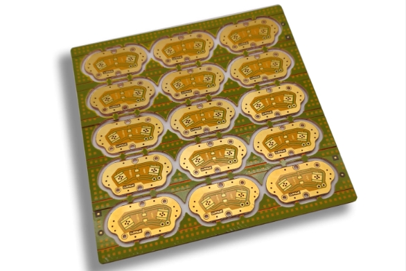
Direct Bonded Copper (DBC) Substrates: Enhancing Electronics with Copper
Definition and Principle of Direct Bonded Copper: Direct bonded copper (DBC) substrates are advanced materials used in electronics manufacturing, featuring a direct bond between a copper layer and a ceramic or metal substrate. The principle behind DBC involves bonding a high-purity copper foil directly onto a base material using a combination of heat, pressure, and sometimes an intermediate bonding layer. This results in a robust interface with excellent thermal and electrical properties, facilitating efficient heat dissipation and signal transmission in electronic devices.
Preparation Process and Key Steps Involved: The preparation of DBC substrates typically involves several key steps. First, the copper foil and the substrate material are thoroughly cleaned to remove any contaminants and ensure proper adhesion. Next, the surfaces to be bonded are activated through methods such as plasma treatment or chemical etching to promote bonding. The copper foil is then placed onto the substrate and subjected to controlled heat and pressure in a bonding press. This process allows the copper to bond directly to the substrate, forming a strong and reliable interface. Optionally, an intermediate bonding layer, such as a solder or adhesive, may be used to enhance bonding strength and thermal conductivity.
Advantages and Applications of Direct Bonded Copper: Direct bonded copper substrates offer numerous advantages in electronic applications. Firstly, they provide superior thermal conductivity compared to traditional printed circuit boards (PCBs), allowing for efficient heat dissipation and enhanced device reliability, particularly in high-power applications such as power electronics and automotive electronics. Additionally, DBC substrates offer excellent electrical conductivity, enabling high-frequency signal transmission with minimal loss. This makes them well-suited for use in radio frequency (RF) and microwave applications, telecommunications equipment, and power amplifiers. Furthermore, DBC substrates exhibit exceptional mechanical strength and dimensional stability, ensuring long-term performance in harsh operating environments. Overall, the versatility, reliability, and performance benefits of DBC substrates make them indispensable components in a wide range of electronic devices, contributing to advancements in technology and innovation.
AMB Substrates: Unveiling the Versatility of Copper Substrates
Characteristics and Applications of AMB Substrates: AMB (Active Metal Brazing) substrates represent a unique class of copper substrates renowned for their exceptional thermal management properties and versatility in diverse electronic applications. These substrates feature a copper base bonded to a ceramic or metal layer using a brazing process, where a metal filler material is melted and solidified to form a strong bond. The resulting AMB substrate exhibits excellent thermal conductivity, allowing efficient dissipation of heat generated by electronic components. This property makes AMB substrates particularly well-suited for high-power applications such as power modules, hybrid electric vehicles, and renewable energy systems where thermal management is critical for device performance and longevity. Additionally, the ability to tailor the composition and thickness of the metal filler material offers flexibility in optimizing thermal and mechanical properties to meet specific application requirements.
Comparison and Pros/Cons Evaluation vis-à-vis Direct Bonded Copper: When comparing AMB substrates to direct bonded copper (DBC), several factors come into play. While both technologies offer superior thermal management capabilities compared to traditional PCBs, they differ in their manufacturing processes and material compositions. AMB substrates typically involve a brazing process, which can offer advantages in terms of bond strength and reliability over the direct bonding process used in DBC substrates. Additionally, the ability to incorporate different filler materials in AMB substrates allows for greater flexibility in optimizing thermal conductivity and mechanical properties. However, the brazing process may introduce additional manufacturing complexity and cost compared to direct bonding. Furthermore, the choice between AMB and DBC substrates depends on specific application requirements, with AMB substrates excelling in high-power applications where precise thermal management is paramount, while DBC substrates may offer advantages in terms of simplicity and cost-effectiveness for certain applications. Ultimately, the selection between AMB and DBC substrates depends on a careful evaluation of performance requirements, cost considerations, and manufacturing capabilities.
Monocrystalline Copper (OCC) Substrates: Elevating Electronics with Pure Copper
Methods of Preparation and Characteristics of Monocrystalline Copper: Monocrystalline copper substrates, also known as OCC substrates, are fabricated using advanced techniques to produce a single, continuous crystal structure with exceptional purity and uniformity. The preparation of OCC substrates typically involves processes such as zone refining or the Czochralski method, which carefully control the solidification of molten copper to form a single crystal ingot. This meticulous process results in a substrate with unparalleled structural integrity and electrical properties. Monocrystalline copper exhibits high electrical conductivity, low electrical resistivity, and excellent thermal conductivity, making it an ideal material for demanding electronic applications where precision and reliability are paramount.
Applications and Advantages of Monocrystalline Copper in the Electronics Industry: Monocrystalline copper substrates find widespread use in various high-performance electronic devices and systems due to their unique combination of properties. In semiconductor manufacturing, OCC substrates serve as ideal platforms for the deposition and integration of thin-film materials, facilitating the fabrication of high-density integrated circuits with enhanced performance and reliability. Moreover, OCC substrates are utilized in radio frequency (RF) and microwave applications, where their superior electrical conductivity enables efficient signal transmission and reception. Additionally, OCC substrates are employed in power electronics, aerospace electronics, and telecommunications equipment, where their exceptional thermal conductivity and mechanical strength ensure reliable operation under harsh conditions. The advantages of OCC substrates extend beyond their electrical and thermal properties, as their single-crystal structure minimizes grain boundaries and defects, contributing to improved device performance and longevity. Overall, monocrystalline copper substrates represent a cornerstone material in the electronics industry, enabling advancements in technology and innovation across various sectors.
Copper Wafer vs. Copper Substrate: Understanding the Differences
Distinctions and Applications: Copper wafers and copper substrates serve distinct purposes in the electronics industry, each with its own set of applications and advantages. Copper wafers are typically thin slices of copper used as substrates for semiconductor device fabrication, such as integrated circuits (ICs) and microelectromechanical systems (MEMS). They provide a flat and conductive surface onto which semiconductor materials are deposited and patterned to create electronic components. Copper substrates, on the other hand, encompass a broader category of copper-based materials used as the foundation for various electronic devices and systems. While copper wafers are primarily utilized in semiconductor manufacturing, copper substrates find applications in PCBs, power electronics, RF/microwave components, and thermal management systems.
Fabrication Processes and Material Properties of Copper Wafers: Copper wafers are typically fabricated using processes similar to those employed in silicon wafer manufacturing, albeit with modifications to accommodate the properties of copper. Initially, high-purity copper ingots are melted and cast into cylindrical shapes, which are then sliced into thin wafers using diamond saws or wire saws. These wafers undergo surface preparation treatments to remove surface contaminants and defects, ensuring optimal adhesion and compatibility with subsequent processing steps. Copper wafers exhibit excellent electrical conductivity and thermal conductivity, making them suitable substrates for semiconductor device fabrication. However, their relatively high cost and susceptibility to oxidation necessitate careful handling and storage to maintain their integrity during manufacturing.
In contrast, copper substrates used in electronic applications may vary in thickness, composition, and surface finish depending on the specific requirements of the intended application. Fabrication processes for copper substrates may involve techniques such as electroplating, etching, or bonding onto other materials to achieve desired properties and dimensions. Copper substrates offer advantages such as high electrical conductivity, excellent thermal conductivity, and mechanical robustness, making them indispensable components in various electronic devices and systems. Additionally, copper substrates are more cost-effective and versatile compared to copper wafers, as they can be customized to meet specific design requirements and accommodate diverse manufacturing processes.
Application Case Studies: Unveiling the Versatility of Copper Substrates
Real-World Application Examples:
- Power Electronics: Direct bonded copper (DBC) substrates are extensively used in power electronic modules for electric vehicles (EVs) and renewable energy systems. These substrates enable efficient heat dissipation, allowing for compact and reliable power converters with enhanced energy efficiency.
- Telecommunications: Monocrystalline copper (OCC) substrates are employed in high-frequency RF/microwave components, such as antennas and amplifiers, where precise signal transmission is critical. The single-crystal structure of OCC substrates minimizes signal loss and distortion, resulting in superior performance.
- Consumer Electronics: Copper wafers are utilized in the fabrication of advanced semiconductor devices, including microprocessors and memory chips, found in smartphones, laptops, and other consumer electronics. The high electrical conductivity of copper wafers enables faster data processing and improved device performance.
Future Development Trends and Potential Applications:
- 5G Technology: With the advent of 5G networks, there is a growing demand for copper substrates in telecommunications infrastructure, particularly for high-speed data transmission and network connectivity. Copper substrates with enhanced thermal and electrical properties will play a crucial role in supporting the rollout of 5G technology.
- Electric Vehicles (EVs): As the automotive industry transitions towards electrification, there is an increasing need for advanced power electronics systems in EVs. Copper substrates capable of handling high currents and temperatures will be essential for the development of efficient and reliable EV powertrains.
- Internet of Things (IoT): The proliferation of IoT devices requires compact and energy-efficient electronic components. Copper substrates with improved thermal management capabilities will enable the development of smaller, more powerful IoT devices with extended battery life.
Copper substrates continue to evolve and find new applications in emerging technologies, driving innovation and progress in the electronics industry. As research and development efforts focus on enhancing the performance and functionality of copper substrates, we can expect to see their widespread adoption across various sectors, further cementing their status as indispensable materials in electronic product design and manufacturing.
FAQs About Copper Substrate
Direct bonded copper (DBC) is a process used in electronics manufacturing where a copper layer is directly bonded to a ceramic or metal substrate. This bonding is achieved through a combination of heat, pressure, and sometimes an intermediate bonding layer, resulting in a strong interface with excellent thermal and electrical properties.
The cubic structure of copper refers to its crystalline arrangement, known as a face-centered cubic (FCC) structure. In this structure, copper atoms are arranged in a regular pattern with each atom surrounded by twelve nearest neighbors. This arrangement contributes to copper’s remarkable mechanical properties and conductivity.
The main difference between Active Metal Brazing (AMB) and Direct Bonded Copper (DBC) substrates lies in their manufacturing processes. AMB substrates involve bonding a copper layer to a ceramic or metal substrate using a brazing process, while DBC substrates utilize direct bonding techniques. Additionally, AMB substrates may incorporate different filler materials to enhance thermal conductivity, while DBC substrates typically feature a pure copper bond.
In electronics, a substrate refers to a base material onto which electronic components or circuits are fabricated or assembled. Substrates provide mechanical support and electrical connections for the components, as well as facilitating heat dissipation and insulation. Common substrate materials include ceramics, metals, and various composite materials, each chosen based on the specific requirements of the electronic device or application.

