
Navigating BGA Substrate Production: Key Phases
Ball Grid Array (BGA) technology revolutionized electronic packaging by enhancing component density and reliability in electronic devices. Unlike traditional through-hole components, BGAs employ an array of solder balls beneath the component, facilitating better thermal conductivity and electrical performance. The substrate, a crucial element in BGA manufacturing, serves as the foundation for mounting integrated circuits and providing electrical connections. Its role extends beyond mere structural support; the substrate’s material composition, design, and manufacturing process significantly impact the overall performance, reliability, and manufacturability of BGA assemblies. Understanding the intricacies of substrate selection and processing is paramount in ensuring the integrity and functionality of BGA-based electronic systems.
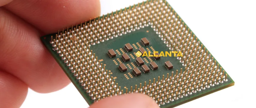
Understanding BGA Production Process
Introduction to BGA Manufacturing Steps:
The production of Ball Grid Array (BGA) components involves several intricate steps to ensure the reliability and functionality of electronic assemblies. The process typically begins with the preparation of the substrate, followed by the placement of solder balls, attachment of integrated circuits, and encapsulation of the assembly. Each step plays a crucial role in the overall manufacturing process, ultimately determining the quality and performance of the BGA component.
Overview of Substrate Preparation:
Substrate preparation is a critical stage in BGA manufacturing, laying the foundation for the assembly of integrated circuits and solder balls. The substrate, often made of materials like fiberglass-reinforced epoxy resin (FR-4) or more advanced materials like ceramic, undergoes several key processes before it’s ready for component mounting:
1. Substrate Fabrication: Initially, raw substrate materials are processed to form thin sheets or panels of precise dimensions. This may involve cutting, laminating, and curing processes to achieve the desired substrate properties.
2. Surface Preparation: The substrate surface is meticulously cleaned and treated to ensure optimal adhesion for subsequent layers and components. This step involves removing any contaminants and applying surface treatments to enhance bonding.
3. Circuit Formation: Circuit patterns, including electrical traces and vias, are created on the substrate surface through processes like etching, printing, or laser ablation. These circuits provide the electrical pathways for connecting the integrated circuits and solder balls.
4. Plating: Metal plating is applied to the substrate’s circuitry to enhance conductivity and solderability. Common plating materials include copper, nickel, and gold, which are deposited onto the substrate surface using techniques like electroplating or electroless plating.
5. Dielectric Layer Deposition: Dielectric layers may be deposited onto the substrate surface to insulate the circuitry and provide mechanical support. These layers help prevent electrical short circuits and ensure the reliability of the BGA assembly.
6. Surface Finish: Finally, the substrate undergoes surface finishing processes to prepare it for solder ball attachment. This may involve applying solder mask layers, which define the areas where solder balls will be attached, and surface treatments to promote solder wetting and bonding.
By meticulously preparing the substrate through these steps, manufacturers ensure the integrity and functionality of BGA components, laying the groundwork for successful electronic assemblies with enhanced reliability and performance.
BGA Manufacturing Process
Solder Ball Placement:
Solder ball placement is a crucial step in BGA manufacturing, as it establishes the electrical and mechanical connections between the integrated circuits and the substrate. The process involves precise placement of solder balls onto predetermined locations on the substrate surface. Several methods may be employed for solder ball deposition:
1. Stencil Printing: A stencil with openings corresponding to the solder ball locations is aligned over the substrate, and solder paste is applied through the stencil openings using a squeegee. The substrate is then heated, causing the solder paste to reflow and form solder balls.
2. Solder Ball Placement Machines: Automated machines equipped with vision systems accurately place individual solder balls onto the substrate’s predefined locations. This method ensures high precision and consistency in solder ball placement.
3. Reflow Soldering: Alternatively, solder balls pre-coated with flux may be placed onto the substrate, and the assembly is subjected to a reflow soldering process. During reflow, the solder balls melt and form secure connections with the substrate and integrated circuits.
Attachment of Integrated Circuits:
After solder ball placement, integrated circuits (ICs) are attached to the substrate, forming the core components of the BGA assembly. This process typically involves the following steps:
1. Die Attach: The ICs, often in the form of semiconductor chips, are precisely positioned over their corresponding locations on the substrate. Adhesive materials, such as epoxy or solder paste, are used to bond the ICs to the substrate surface.
2. Wire Bonding: Thin wires made of gold or aluminum are then used to establish electrical connections between the ICs and the substrate’s circuitry. Wire bonding techniques, including wedge bonding and ball bonding, are employed to securely bond the wires to the IC pads and substrate traces.
3. Underfill Encapsulation: To enhance the mechanical strength and reliability of the IC connections, an underfill material may be applied between the IC and substrate. This encapsulation material flows into the gaps between the IC and substrate, providing additional support and stress relief during thermal cycling and mechanical stresses.
Substrate Encapsulation:
Substrate encapsulation is the final step in BGA manufacturing, providing protection and stability to the assembled components. The encapsulation process involves:
1. Mold Encapsulation: The entire BGA assembly, including the substrate, solder balls, and attached ICs, is encapsulated within a protective mold compound. This compound is typically an epoxy resin that is injected or dispensed around the assembly and cured to form a solid, protective shell.
2. Curing: The encapsulated BGA assembly is subjected to heat or UV radiation to cure the mold compound, ensuring proper adhesion and structural integrity. Curing also helps to remove any remaining moisture and solvents from the encapsulant.
Once encapsulated, the BGA assembly undergoes testing and inspection to verify its functionality and reliability before being integrated into electronic devices. The encapsulation process not only protects the components from environmental factors but also provides mechanical reinforcement, ensuring the long-term performance of BGA-based electronic systems.
Exploring BGA Substrate
Definition and Role of Substrate in BGA Technology:
In Ball Grid Array (BGA) technology, the substrate serves as the foundation upon which integrated circuits (ICs) are mounted and interconnected. It plays a critical role in facilitating the electrical and mechanical connections between the ICs and the printed circuit board (PCB) or motherboard of the electronic device. The substrate provides a stable platform for the attachment of ICs and serves as a medium for routing electrical signals between the ICs and other components.
The substrate acts as a host for the solder balls that connect the ICs to the PCB. It also provides support for the ICs and ensures proper alignment during assembly. Additionally, the substrate helps dissipate heat generated by the ICs, contributing to the thermal management of the electronic system. Overall, the substrate is essential for maintaining the structural integrity, electrical connectivity, and thermal performance of BGA-based electronic assemblies.
Types of Substrates Used in BGA Manufacturing:
Several types of substrates are commonly used in BGA manufacturing, each offering distinct properties and advantages suited to specific application requirements. Some of the most commonly used substrate materials include:
1. FR-4 (Fiberglass-Reinforced Epoxy): FR-4 is a widely used substrate material known for its affordability, ease of fabrication, and good electrical insulation properties. It consists of a woven fiberglass core impregnated with epoxy resin, providing mechanical strength and dimensional stability.
2. Polyimide: Polyimide substrates offer excellent thermal stability, flexibility, and resistance to moisture and chemicals. These substrates are commonly used in applications requiring high-temperature operation and flexibility, such as flexible PCBs and high-density interconnects.
3. Ceramic: Ceramic substrates, typically made of alumina (Al2O3) or aluminum nitride (AlN), offer superior thermal conductivity and mechanical strength compared to organic substrates. Ceramic substrates are ideal for high-power and high-frequency applications where efficient heat dissipation and reliability are critical.
4. Metal-Core PCB (MCPCB): MCPCBs feature a metal core, usually aluminum or copper, sandwiched between layers of dielectric material. These substrates offer excellent thermal conductivity, making them suitable for applications requiring efficient heat dissipation, such as LED lighting and power electronics.
5. Flexible Substrates: Flexible substrates, made of materials like polyimide or polyester, offer flexibility and bendability, making them ideal for applications requiring compact and lightweight designs, such as wearable devices and flexible displays.
By selecting the appropriate substrate material and design, manufacturers can optimize the performance, reliability, and manufacturability of BGA-based electronic assemblies, meeting the diverse requirements of various applications.
FC BGA Manufacturing Process
Introduction to Flip Chip (FC) BGA Technology:
Flip Chip (FC) BGA technology is an advanced packaging technique that offers numerous advantages over traditional BGA assembly methods. In FC BGA, the semiconductor chip is flipped upside down and directly mounted onto the substrate, allowing for shorter interconnection lengths and improved electrical performance. Unlike traditional wire bonding, FC BGA uses solder bumps to establish electrical connections between the chip and the substrate, resulting in higher packaging densities and enhanced signal integrity.
Key Differences Between FC BGA and Traditional BGA Manufacturing Processes:
1. Interconnection Method: In traditional BGA manufacturing, wire bonding is typically used to establish electrical connections between the semiconductor chip and the substrate. In contrast, FC BGA utilizes solder bumps or balls for direct chip-to-substrate connections, eliminating the need for wire bonding and reducing interconnection lengths.
2. Package Size and Density: FC BGA technology allows for smaller package sizes and higher packaging densities compared to traditional BGA assemblies. By eliminating the need for wire bonds, FC BGA enables tighter chip-to-chip spacing and greater integration of components, making it ideal for high-density electronic applications.
3. Thermal Management: FC BGA offers improved thermal performance compared to traditional BGA assemblies due to shorter interconnection lengths and enhanced heat dissipation through the solder bumps. This allows for better thermal management and reliability in high-power applications.
4. Signal Integrity: The shorter interconnection lengths in FC BGA result in reduced signal propagation delays and improved signal integrity, making it suitable for high-speed and high-frequency applications. Additionally, the direct chip-to-substrate connections minimize parasitic effects, further enhancing signal quality.
Step-by-Step Guide to FC BGA Production:
1. Substrate Preparation: The substrate undergoes the same preparation steps as in traditional BGA manufacturing, including fabrication, surface preparation, circuit formation, plating, and surface finishing.
2. Solder Bump Deposition: Solder bumps are deposited onto the bonding pads of the semiconductor chip using techniques such as solder jetting, stencil printing, or electroplating. The solder bumps serve as the interconnection points between the chip and the substrate.
3. Die Attach: The semiconductor chip is flipped upside down and precisely aligned over the substrate, with the solder bumps facing downward. An adhesive material is used to bond the chip to the substrate surface.
4. Reflow Soldering: The assembly undergoes reflow soldering to melt the solder bumps and establish electrical connections between the chip and the substrate. The reflow process ensures proper alignment and bonding of the chip to the substrate.
5. Underfill Encapsulation: An underfill material may be applied between the chip and the substrate to provide mechanical support and enhance reliability. The underfill material flows into the gaps between the chip and the substrate, reinforcing the solder joints and reducing mechanical stresses.
6. Substrate Encapsulation: Finally, the entire FC BGA assembly is encapsulated within a mold compound to provide protection and stability. The encapsulation process involves injecting or dispensing the mold compound around the assembly and curing it to form a solid, protective shell.
By following these steps, manufacturers can produce FC BGA assemblies with enhanced performance, reliability, and packaging density, making them suitable for a wide range of advanced electronic applications.
FAQs about bga substrate process flow
BGA production involves several steps, including substrate preparation, solder ball placement, attachment of integrated circuits, and encapsulation of the assembly. These steps ensure the creation of reliable and functional BGA components.
The BGA manufacturing process includes substrate preparation, solder ball placement, attachment of integrated circuits to the substrate, and encapsulation of the assembled components. These steps are meticulously executed to ensure the quality and performance of the BGA components.
In BGA technology, the substrate serves as the foundation upon which integrated circuits are mounted and interconnected. It provides structural support, electrical connectivity, and thermal management for the BGA assembly.
The manufacturing process of FC BGA (Flip Chip Ball Grid Array) involves substrate preparation, deposition of solder bumps on the semiconductor chip, attachment of the chip to the substrate using adhesive, reflow soldering to establish electrical connections, application of underfill for mechanical support, and encapsulation of the assembly. This process enables the creation of high-density, high-performance BGA assemblies with improved thermal and electrical

