
IC Substrate PCBs: Engineered for Advanced Integration
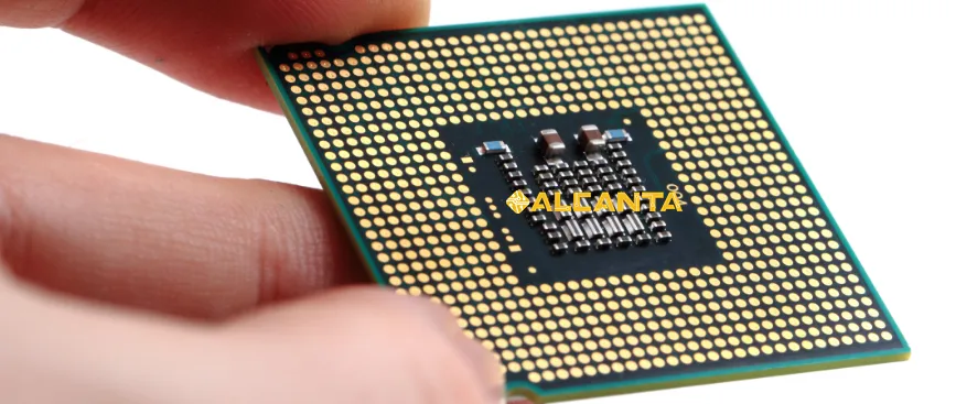
Introduction: Integrated Circuit (IC) Substrate PCBs play a pivotal role in modern electronics by providing a specialized foundation for semiconductor packaging. Unlike traditional PCBs, IC Substrate PCBs are engineered with materials like High Temperature Co-Fired Ceramic (HTCC) or Low Temperature Co-Fired Ceramic (LTCC) to meet stringent requirements of miniaturization, thermal management, and electrical performance crucial for ICs. Their significance lies in enhancing the reliability, performance, and functionality of integrated circuits, making them indispensable in applications ranging from telecommunications infrastructure to advanced automotive electronics and consumer devices. Understanding IC Substrate PCBs is essential for grasping how cutting-edge technologies are integrated and optimized, driving innovation in the rapidly evolving semiconductor industry.
Difference Between IC Substrate PCBs and Standard PCBs
IC Substrate PCBs differ significantly from standard Printed Circuit Boards (PCBs) in both construction and function:
Construction and Material Composition
IC Substrate PCBs are typically constructed using specialized materials such as High Temperature Co-Fired Ceramic (HTCC) or Low Temperature Co-Fired Ceramic (LTCC). These materials offer superior thermal conductivity, mechanical strength, and electrical performance compared to standard FR-4 or epoxy-based PCB substrates. The construction often includes multiple layers of conductive traces and vias, optimized for high-density interconnections required by integrated circuits.
Functionality and Integration
IC Substrate PCBs play a critical role in integrated circuit packaging by providing a robust platform for mounting and interconnecting semiconductor devices. Unlike standard PCBs, which primarily serve as a mechanical support and electrical interconnect, IC Substrate PCBs are designed to manage heat dissipation effectively, ensure signal integrity at high frequencies, and minimize parasitic effects that could degrade circuit performance.
Crucial Role in Integrated Circuit Packaging
The integration of ICs onto specialized substrates facilitates advanced packaging techniques such as flip-chip, wire bonding, and stacked die configurations. This integration enhances the overall reliability and performance of integrated circuits, making IC Substrate PCBs essential for applications demanding high-speed data processing, compact form factors, and reliability in harsh environments.
Understanding these distinctions underscores the importance of IC Substrate PCBs in modern electronics, where efficiency, miniaturization, and performance are paramount in driving technological advancements.
Manufacturing Process of IC Substrates
The manufacturing of IC Substrates involves several intricate processes tailored to meet the stringent requirements of integrated circuit packaging:
Processes Involved in IC Substrate Production
1. Substrate Preparation: The process begins with the selection and preparation of specialized materials such as High Temperature Co-Fired Ceramic (HTCC) or Low Temperature Co-Fired Ceramic (LTCC). These materials are formulated to provide high thermal conductivity, mechanical stability, and excellent electrical properties.
2. Layer Formation: Multiple layers of ceramic or organic substrates are fabricated through processes like tape casting or screen printing. Each layer is designed to accommodate conductive traces, vias, and bonding pads necessary for IC attachment.
3. Conductor Patterning: Conductive patterns are created using techniques such as thin-film deposition, screen printing of conductive pastes, or laser ablation. These patterns define the electrical pathways that connect different components of the integrated circuit.
4. Via Formation: Vias are drilled or formed to establish vertical interconnections between different layers of the substrate. Advanced techniques like laser drilling ensure precise alignment and minimal thermal impact on the substrate material.
5. Metallization and Bonding Pad Formation: Metal layers are deposited and patterned to form bonding pads and interconnects. These pads provide contact points for attaching semiconductor devices using methods like wire bonding or flip-chip bonding.
6. Assembly and Testing: Once the substrate layers are prepared and metallized, semiconductor devices are assembled onto the substrate using automated placement equipment. The assembled substrates undergo rigorous testing to ensure electrical functionality and reliability.
Key Materials and Manufacturing Techniques
– Materials: HTCC and LTCC ceramics are favored for their thermal management capabilities and electrical performance. Organic substrates like BT (Bismaleimide Triazine) are also used for their mechanical flexibility and compatibility with high-speed signal transmission.
– Manufacturing Techniques: Techniques such as tape casting, screen printing, laser ablation, and thin-film deposition are critical in forming substrate layers, conductive traces, and vias with high precision and reliability.
Understanding these manufacturing processes and materials highlights the complexity and precision involved in producing IC Substrates, essential for enabling advanced packaging solutions in modern integrated circuits.
Types of IC Substrates
There are several types of IC Substrates, each tailored to specific requirements of integrated circuit packaging and performance:
High Temperature Co-Fired Ceramic (HTCC)
HTCC substrates are manufactured using ceramic materials that can withstand high temperatures during processing and operation. These substrates offer excellent thermal conductivity, mechanical strength, and reliability, making them suitable for high-power applications and harsh environments.
Low Temperature Co-Fired Ceramic (LTCC)
LTCC substrates are processed at lower temperatures compared to HTCC, using ceramic materials that exhibit good electrical properties and dimensional stability. LTCC substrates are valued for their miniaturization capabilities and are often used in RF/microwave applications and sensors.
High-Density Interconnect (HDI)
HDI substrates incorporate advanced manufacturing techniques to achieve high-density interconnections between layers. These substrates feature microvia technology, fine-line circuitry, and multiple layers to accommodate complex circuit designs. HDI substrates are essential for compact, high-performance electronic devices such as smartphones, tablets, and wearables.
Organic Substrates (e.g., BT)
Organic substrates, such as Bismaleimide Triazine (BT), offer flexibility and cost-effectiveness while maintaining good electrical performance and thermal stability. They are widely used in high-speed digital applications where signal integrity and reliability are critical.
Flexible Substrates
Flexible substrates are composed of flexible materials like polyimide or polyester. These substrates are ideal for applications requiring bendability or conformal properties, such as flexible displays, RFID antennas, and medical devices.
Composite Substrates
Composite substrates combine different materials to achieve specific performance characteristics, such as enhanced thermal management or mechanical properties. These substrates are tailored for demanding applications in aerospace, automotive, and industrial electronics.
Each type of IC substrate offers unique advantages suited to diverse applications in modern electronics, highlighting the importance of selecting the right substrate to optimize performance, reliability, and manufacturability of integrated circuits.
Applications of IC Substrates
IC Substrates find extensive applications across various industries, leveraging their specialized properties to enhance performance and reliability in critical electronic systems:
Telecommunications
IC Substrates play a crucial role in telecommunications infrastructure, where they are used in RF/microwave components, base station equipment, and satellite communications systems. High-performance substrates like HTCC and LTCC enable efficient signal processing, low-loss transmission, and reliability in challenging environmental conditions.
Automotive Electronics
In automotive electronics, IC Substrates support advanced driver assistance systems (ADAS), engine control units (ECUs), and infotainment systems. HTCC and LTCC substrates provide thermal management, vibration resistance, and durability required for automotive applications, ensuring reliable operation under harsh temperatures and mechanical stress.
Consumer Electronics
Consumer electronics benefit from IC Substrates in devices such as smartphones, tablets, and wearables. HDI substrates enable miniaturization, high-speed data transmission, and compact design layouts essential for enhancing device performance, battery life, and user experience.
Medical Devices
IC Substrates are essential in medical devices for applications like patient monitoring systems, diagnostic equipment, and implantable devices. Flexible and bio-compatible substrates support conformal designs, biocompatibility, and reliable performance critical in medical environments.
Aerospace and Defense
In aerospace and defense sectors, IC Substrates are used in radar systems, avionics, and military communications. Composite substrates offer lightweight solutions with high thermal conductivity and mechanical strength, meeting stringent requirements for reliability, ruggedness, and performance in extreme environments.
Industrial Electronics
Industrial applications utilize IC Substrates in control systems, robotics, and industrial automation. Substrates with enhanced thermal management and ruggedized designs ensure long-term reliability and operational stability in industrial settings.
Emerging Technologies
IC Substrates also support emerging technologies such as Internet of Things (IoT), 5G infrastructure, and augmented reality (AR)/virtual reality (VR) devices. These applications benefit from substrates that enable high-speed data processing, connectivity, and integration of advanced functionalities.
The versatile applications of IC Substrates underscore their importance in enabling technological advancements across diverse industries, driving innovation in electronic systems and enhancing capabilities in critical applications.
Connection Between IC Substrate and PCB
IC Substrates and traditional Printed Circuit Boards (PCBs) serve distinct yet complementary roles in electronic systems, particularly in integrated circuit (IC) packaging:
Relationship and Distinctions
IC Substrates are specialized substrates designed specifically for mounting and interconnecting semiconductor devices. Unlike traditional PCBs, which serve as a platform for mounting various electronic components and providing electrical connections, IC Substrates are optimized for the unique requirements of IC packaging. They incorporate materials like High Temperature Co-Fired Ceramic (HTCC), Low Temperature Co-Fired Ceramic (LTCC), or advanced organic substrates to meet stringent performance criteria such as thermal management, signal integrity, and miniaturization.
Unique Role of IC Substrate PCBs in IC Packaging
IC Substrate PCBs play a critical role in enhancing the reliability and performance of integrated circuits. They provide a robust foundation for mounting ICs using advanced packaging techniques such as flip-chip bonding, wire bonding, or through-silicon via (TSV) technology. The substrate’s design includes intricate patterns of conductive traces, vias, and bonding pads tailored to the specific requirements of each IC package. This design optimization minimizes signal loss, reduces electromagnetic interference (EMI), and enhances thermal dissipation capabilities, which are crucial for maintaining IC functionality and longevity.
By integrating IC Substrates into PCB assemblies, manufacturers can achieve compact, high-density designs that optimize space, improve electrical performance, and meet the increasing demands of modern electronic devices. This integration highlights the synergy between IC Substrate technology and traditional PCB manufacturing processes, enabling innovations in IC packaging and advancing electronic system capabilities across industries.
Future Trends of IC Substrates
The future of IC Substrates is poised for significant advancements driven by technological innovations and evolving industry demands:
Directions in IC Substrate Development
1. Miniaturization and Integration: Future IC Substrates will focus on further miniaturization to accommodate smaller form factors and higher integration densities. This trend is crucial for applications in mobile devices, IoT sensors, and wearable electronics.
2. Advanced Materials: Continued research into new materials with enhanced thermal conductivity, electrical performance, and mechanical properties will expand the capabilities of IC Substrates. Materials like graphene and advanced ceramics hold promise for improving substrate efficiency and reliability.
3. High-Frequency Applications: As the demand for high-speed data processing and communication grows, IC Substrates will need to support higher frequencies and reduced signal losses. Advances in substrate design and manufacturing will optimize signal integrity and minimize electromagnetic interference.
Technological Trends in IC Substrate Development
1. Embedded Components: Integration of passive components, such as resistors and capacitors, directly into IC Substrates will streamline assembly processes, reduce footprint, and enhance electrical performance.
2. 3D Packaging Technologies: Adoption of advanced packaging techniques like 3D stacking, System-in-Package (SiP), and Through-Silicon Vias (TSVs) will enable complex multi-functional devices with improved performance and efficiency.
3. Flexible and Stretchable Substrates: Development of flexible and stretchable IC Substrates using innovative materials and manufacturing techniques will drive advancements in wearable electronics, biomedical devices, and conformal electronics.
Innovations and Application Prospects
1. 5G and Beyond: IC Substrates will play a pivotal role in supporting the rollout of 5G networks by enabling high-frequency RF/microwave components and compact antenna designs. Future applications may include mmWave technologies and beyond.
2. Artificial Intelligence (AI) and Edge Computing: AI-driven applications and edge computing devices will benefit from IC Substrates optimized for high-performance computing, low power consumption, and efficient thermal management.
3. Environmental Sustainability: Development of eco-friendly materials and manufacturing processes will address sustainability concerns in electronics manufacturing, promoting recyclability and reducing environmental impact.
The future of IC Substrates is marked by continuous innovation and adaptation to meet the evolving needs of diverse industries. Advancements in materials, packaging technologies, and application-specific designs will drive the next generation of electronic devices, shaping the future landscape of IC Substrate development and deployment.
FAQs about ic substrate pcb
IC substrate PCB refers to a specialized type of Printed Circuit Board (PCB) designed to provide a foundation for mounting and interconnecting integrated circuits (ICs). It incorporates materials and design features optimized for the specific requirements of IC packaging, such as thermal management, signal integrity, and electrical performance.
The substrate of ICs is the physical base or foundation on which the integrated circuit is mounted and interconnected. It provides mechanical support and electrical connections for the IC, typically made from materials like silicon, ceramic, or organic materials such as BT (Bismaleimide Triazine).
The primary function of the IC substrate is to provide a stable platform for mounting the IC and facilitating electrical connections between the IC and other components or circuits. It also helps dissipate heat generated by the IC, ensures signal integrity, and minimizes electromagnetic interference (EMI), thereby enhancing the overall performance and reliability of the integrated circuit.
In the context of a PCB, IC stands for Integrated Circuit. It refers to a miniature electronic circuit consisting of semiconductor devices, passive components (resistors, capacitors), and interconnections (metal traces) fabricated on a single semiconductor substrate. ICs perform various functions ranging from amplification, signal processing, to digital logic operations within electronic devices.

