
PCB Substrates: Materials and Structural Insights
The Printed Circuit Board (PCB) is an indispensable component in modern electronic products, serving as the foundation for electronic circuits and providing the mechanical support and electrical connections essential for the operation of various devices. At the heart of PCB technology lies its substrate, a critical element that influences the board’s performance, durability, and suitability for different applications. Substrate technology encompasses a range of materials and structures, each tailored to meet specific requirements in terms of thermal stability, electrical insulation, and mechanical strength. Understanding the various types of PCB substrates, their materials, and structural nuances is crucial for optimizing electronic designs and ensuring the reliability of the end products. As technology continues to evolve, advancements in substrate technology are paving the way for more sophisticated and efficient electronic solutions, highlighting the ongoing importance of innovation in this field.
Types of PCB Substrates
FR4 Substrates
FR4 is the most common type of PCB substrate, known for its flame retardant properties. It consists of a woven fiberglass cloth impregnated with an epoxy resin binder. FR4 substrates offer excellent electrical insulation, mechanical strength, and dimensional stability. They are widely used in consumer electronics, telecommunications, and industrial applications due to their cost-effectiveness and versatility.
Substrate-Like PCB (SLP)
SLP, or Substrate-Like PCB, is a newer type of substrate that aims to provide high performance in a thinner and lighter package compared to traditional FR4 boards. SLP substrates often use materials like liquid crystal polymer (LCP) or other advanced materials with low dielectric loss and excellent high-frequency performance. They are suitable for high-density interconnects (HDI) and applications requiring high-speed signal transmission, such as mobile devices and telecommunications infrastructure.
Other Types
Other types of PCB substrates include ceramic substrates, metal core PCBs (MCPCB), and flexible PCBs (FPC). Ceramic substrates are used in high-power and high-frequency applications due to their excellent thermal conductivity. MCPCBs have a metal core (typically aluminum or copper), providing better heat dissipation, making them ideal for LED lighting and power electronics. FPCs offer flexibility and are used in applications where bending or twisting is required, such as wearable devices and medical equipment. Each type of substrate offers unique characteristics suited to specific electronic design requirements.
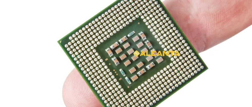
Differences between IC Substrates and PCBs
Design
Integrated Circuit (IC) substrates are specifically designed to support the integration and connection of semiconductor devices (chips). They are optimized for high-density interconnects and often incorporate advanced materials to meet stringent electrical and thermal performance requirements. IC substrates typically have complex wiring patterns and may include features like embedded passives and through-silicon vias (TSVs).
In contrast, PCBs are designed to provide electrical connections between various components, including ICs, resistors, capacitors, and connectors. They are more versatile in terms of their design flexibility and can accommodate a wide range of electronic components and technologies.
Usage
IC substrates are primarily used for packaging and connecting semiconductor chips. They provide the necessary electrical connections and thermal management for the integrated circuits, ensuring reliable operation and performance. IC substrates are crucial in applications requiring high-speed signal transmission and miniaturization, such as microprocessors, memory modules, and high-performance computing devices.
PCBs, on the other hand, are used as the base platform for assembling and interconnecting various electronic components. They provide mechanical support and electrical pathways for components and are used in almost all electronic devices, ranging from smartphones and computers to automotive electronics and industrial equipment.
Manufacturing Processes
The manufacturing processes for IC substrates and PCBs differ significantly. IC substrates often involve more complex and specialized processes, such as thin-film deposition, photolithography, and advanced packaging techniques (e.g., flip-chip bonding, chip-on-board). These processes are designed to ensure precise alignment and electrical performance for integrated circuits.
PCBs are manufactured using techniques such as etching, drilling, and layer stacking. They are more standardized in terms of manufacturing processes and can be produced in high volumes using automated assembly lines. PCB manufacturing focuses on ensuring reliable electrical connectivity and mechanical robustness at a competitive cost.
In summary, while both IC substrates and PCBs serve as critical components in electronic systems, their design, usage, and manufacturing processes are tailored to meet different requirements and applications in the electronics industry.
PCB Substrate Materials
FR4
FR4 is the most widely used PCB substrate material. It consists of a woven fiberglass cloth impregnated with an epoxy resin binder. FR4 substrates are known for their excellent electrical insulation properties, mechanical strength, and dimensional stability. They offer good chemical resistance and are relatively inexpensive compared to other materials. FR4 is suitable for a wide range of applications, including consumer electronics, telecommunications, and industrial equipment.
Metal Core PCB (MCPCB)
Metal Core PCBs (MCPCBs) have a metal core (typically aluminum or copper) that provides enhanced thermal conductivity. This feature makes MCPCBs ideal for applications requiring efficient heat dissipation, such as LED lighting, power electronics, and automotive electronics. The metal core also provides mechanical strength and rigidity, making MCPCBs more robust compared to standard FR4 boards.
Ceramic Substrates
Ceramic substrates are used in high-power and high-frequency applications due to their excellent thermal conductivity, low thermal expansion coefficient, and high electrical insulation properties. Ceramic substrates can be made from materials such as alumina (Al2O3) or aluminum nitride (AlN). They are suitable for applications in RF/microwave devices, power amplifiers, and high-speed digital circuits.
Flexible PCBs (FPC)
Flexible PCBs (FPCs) are made from flexible materials like polyimide. They are lightweight, compact, and can be bent or twisted to fit into tight spaces or conform to complex shapes. FPCs are used in applications where flexibility or dynamic movement is required, such as wearable devices, medical equipment, and aerospace applications. They offer good thermal stability and resistance to vibration and shock.
Other Materials
Other PCB substrate materials include high-frequency laminates (e.g., PTFE-based materials) for applications requiring excellent signal integrity at high frequencies, and composite materials like liquid crystal polymer (LCP) for high-density interconnects (HDI) and mobile device applications.
Each PCB substrate material has unique characteristics that make it suitable for specific applications, depending on factors such as thermal management requirements, electrical performance, mechanical strength, and cost considerations. Choosing the right substrate material is critical for ensuring the reliability and performance of electronic devices and systems.
PCB Substrate Structure
Printed Circuit Boards (PCBs) consist of multiple layers that serve different purposes and are essential for the functionality and performance of electronic devices.
Inner Layers
Inner layers of a PCB typically consist of a core material, such as FR4, sandwiched between layers of copper foil. The copper layers are etched to create circuit patterns that interconnect different components on the board. Inner layers provide the main electrical pathways and connections between components. They may also include additional layers for power and ground planes, which help distribute power and reduce electromagnetic interference (EMI).
Outer Layers
Outer layers of a PCB consist of copper foil bonded to the surface of the substrate material. Like inner layers, these layers are etched to create circuit patterns, but they are accessible from the exterior of the PCB for component mounting and soldering. Outer layers typically include signal traces, which carry electrical signals between components, and may also include solder mask and silkscreen layers for protection and component identification.
Metal Layers
PCBs may include additional metal layers beyond the copper layers used for circuit routing. These metal layers are often used for specific purposes such as shielding, heat dissipation, or as part of the ground plane to provide a low-impedance return path for currents. Metal layers can be made of copper, aluminum, or other conductive materials depending on the requirements of the PCB design.
Functions and Design Considerations
– Signal Routing: The primary function of PCB layers is to provide pathways for electrical signals between components. Signal traces must be carefully routed to minimize signal degradation and interference.
– Power and Ground Planes: Power planes distribute voltage to components and provide a low-impedance path for return currents. Ground planes help reduce noise and EMI and provide a reference voltage for signal integrity.
– Thermal Management: Metal layers and thermal vias are used for heat dissipation, transferring heat away from heat-sensitive components to ensure reliable operation.
– Mechanical Support: The substrate material and its layering provide mechanical support and rigidity to the PCB, ensuring that components are securely mounted and the board can withstand mechanical stresses.
– Manufacturability: Design considerations include the ease of manufacturing, such as the alignment of layers during lamination, and the ability to ensure consistent and reliable electrical connectivity across the board.
Understanding the layered structure of PCBs and the functions of each layer is crucial for designing and manufacturing PCBs that meet the electrical, thermal, and mechanical requirements of various applications.
Coefficient of Thermal Expansion (CTE) of PCB
The Coefficient of Thermal Expansion (CTE) is a critical parameter that affects the performance and reliability of Printed Circuit Boards (PCBs), particularly in environments where temperature variations are significant.
Impact on Performance and Reliability
The CTE of a PCB substrate determines how much the material will expand or contract with changes in temperature. When a PCB is subjected to temperature cycling (heating and cooling), materials with different CTEs can expand or contract at different rates. This can lead to mechanical stress, which may cause delamination of PCB layers, solder joint failures, or even cracks in the substrate or components.
High CTE mismatches between the PCB substrate and components can result in reliability issues, such as intermittent electrical connections or outright failure. Therefore, choosing a PCB substrate with a CTE that closely matches that of the components and the assembly environment is crucial for ensuring long-term reliability.
Choosing Suitable Substrate Materials
To mitigate the effects of CTE on PCB performance and reliability, several strategies can be employed:
– Material Selection: Select PCB substrate materials with CTE values that are compatible with the components and assembly processes. For example, FR4 has a relatively high CTE (around 14-18 ppm/°C), which is suitable for many applications. For high-temperature applications or where low CTE mismatch is critical, materials like ceramic (Alumina or Aluminum Nitride) with lower CTE values (around 6-8 ppm/°C for Alumina) may be more appropriate.
– Design Considerations: Design PCBs with a balanced layer stackup to minimize CTE-induced stress. This includes ensuring symmetrical layer construction, using balanced copper distribution, and avoiding large differences in CTE between adjacent layers.
– Thermal Management: Implement effective thermal management techniques, such as thermal vias and heat sinks, to dissipate heat and reduce temperature gradients across the PCB.
– Testing and Validation: Perform thorough thermal cycling tests and reliability assessments to evaluate the PCB’s performance under expected operating conditions.
In summary, understanding the CTE characteristics of PCB substrate materials and their impact on assembly reliability is essential for selecting materials and designing PCBs that meet the performance and reliability requirements of electronic devices.
Substrate-Like PCB (SLP)
Substrate-Like PCB (SLP) is a relatively new type of PCB substrate that offers significant advantages over traditional substrates like FR4 in terms of size, weight, and performance.
Characteristics
SLP is typically constructed using advanced materials such as liquid crystal polymer (LCP) or other high-performance dielectric materials. These materials provide excellent electrical properties, including low dielectric loss and high signal integrity, making SLP ideal for high-frequency and high-speed applications.
The manufacturing process for SLP involves embedding very thin copper foil layers within the dielectric material, creating a substrate that behaves more like the integrated circuit (IC) itself rather than a standard PCB. This construction allows for a thinner and lighter board compared to FR4, reducing the overall size and weight of electronic devices.
SLP also supports very fine pitch technology, enabling denser interconnects and smaller vias, which are crucial for modern electronic devices where miniaturization and high-density packaging are essential.
Application Areas
SLP is particularly well-suited for applications requiring:
– High-Frequency Performance: SLP’s low dielectric loss and high signal integrity make it ideal for applications operating at high frequencies, such as 5G telecommunications equipment, radar systems, and high-speed data transmission devices.
– Miniaturization: Due to its thin profile and ability to support fine pitch technology, SLP is used in compact electronic devices where space is limited, including smartphones, tablets, and wearable devices.
– High-Density Interconnects (HDI): SLP’s construction allows for multiple layers of very thin copper, facilitating complex, high-density interconnects necessary for advanced electronic designs.
– Advanced Packaging: SLP is increasingly used in advanced packaging applications, including System-in-Package (SiP) and Multi-Chip Modules (MCM), where integrating multiple functions into a single package is critical.
Benefits
– Size and Weight Reduction: SLP’s thin profile and lightweight construction contribute to reducing the overall size and weight of electronic devices, which is crucial for portable devices and applications requiring miniaturization.
– Improved Electrical Performance: SLP’s high-frequency capabilities and low loss characteristics improve signal integrity and reduce electromagnetic interference (EMI), enhancing the overall performance of electronic systems.
In summary, SLP represents a significant advancement in PCB substrate technology, offering enhanced electrical performance, miniaturization capabilities, and versatility for a wide range of high-frequency and high-density applications.
FAQs about substrate pcb
The substrate of a PCB (Printed Circuit Board) refers to the base material that provides mechanical support and electrical insulation for the components and traces on the board. It is the foundation upon which the copper traces are laminated and etched.
The main differences between IC (Integrated Circuit) substrates and PCBs lie in their design, usage, and manufacturing processes. IC substrates are specifically designed to house and interconnect semiconductor chips, often using materials and technologies optimized for high-density interconnects and thermal management. PCBs, on the other hand, are more versatile and are used to connect various electronic components, including ICs, resistors, capacitors, etc., using standardized manufacturing processes.
Yes, FR4 is a type of substrate commonly used in PCBs. It consists of a woven fiberglass cloth impregnated with an epoxy resin binder. FR4 is known for its electrical insulation properties, mechanical strength, and cost-effectiveness, making it one of the most widely used substrate materials in the industry.
Substrate height in PCB refers to the thickness of the PCB substrate material. It is the distance between the top and bottom surfaces of the PCB. Substrate height is an important design parameter as it influences the overall mechanical dimensions of the PCB, the ability to dissipate heat, and the board’s resistance to warping or bending.

