
Maximizing Efficiency: PoP Assembly in Electronics
The semiconductor industry has witnessed a remarkable evolution in packaging technology, driven by the incessant quest for miniaturization, performance enhancement, and system integration. Amidst this evolution, Package on Package (PoP) assembly emerges as a pioneering technique, heralding a new era of compact, high-performance integrated circuits. PoP revolutionizes traditional packaging methods by vertically stacking multiple IC packages, thereby maximizing space efficiency and enabling unprecedented levels of functionality within a constrained footprint. This innovative approach holds profound significance in the semiconductor landscape, offering a paradigm shift in enhancing the performance, functionality, and versatility of integrated circuits across diverse applications. As we delve deeper into the realm of PoP assembly, we uncover its transformative potential in shaping the future of electronics, driving innovation, and redefining the boundaries of what’s possible in semiconductor packaging.
Understanding Package on Package (PoP) Assembly
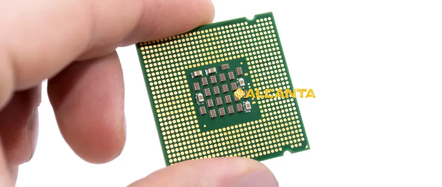
Package on Package (PoP) assembly is a cutting-edge packaging technique that involves vertically stacking multiple IC packages on top of each other, thereby creating a compact and highly integrated system. In PoP assembly, a primary package containing the main logic or processing unit is mounted directly onto a substrate or motherboard. On top of this primary package, a secondary package, typically comprising memory components, is stacked using interconnects such as solder balls or microbumps.
PoP’s architecture differs significantly from traditional packaging methods in several key aspects. Unlike conventional single-package solutions where all components are housed within a single package, PoP separates critical components into distinct layers, enabling greater flexibility, scalability, and performance optimization. This modular approach facilitates easier upgrades or replacements of individual components without requiring extensive rework of the entire system.
The advantages of PoP assembly are manifold. Firstly, PoP enables a significant reduction in footprint by vertically stacking components, thereby conserving valuable board space and allowing for more compact device designs. This space-saving feature is particularly crucial in applications where size constraints are paramount, such as mobile devices and wearable electronics.
Moreover, PoP assembly offers improved electrical performance by minimizing signal transmission distances between the processor and memory components. With shorter interconnect lengths, PoP mitigates signal degradation, reduces latency, and enhances data transfer speeds, resulting in superior system responsiveness and overall performance.
Furthermore, PoP facilitates increased system integration by accommodating multiple functions within a single package assembly. By stacking logic and memory components vertically, PoP enables seamless integration of diverse functionalities, such as computing, storage, and connectivity, into a unified system, thereby streamlining the overall design and enhancing efficiency.
In essence, Package on Package (PoP) assembly represents a groundbreaking advancement in semiconductor packaging, offering unparalleled levels of miniaturization, performance, and functionality. Its unique architecture, coupled with a host of benefits including reduced footprint, improved electrical performance, and increased system integration, positions PoP as a cornerstone technology driving innovation across a wide range of electronic applications.
The Use and Applications of Package on Package (PoP)
Package on Package (PoP) assembly has emerged as a versatile and indispensable technology, finding widespread adoption across a myriad of industries due to its unique advantages and capabilities.
Diverse Applications:
PoP assembly finds extensive use in a diverse range of applications, with notable prominence in mobile devices, IoT gadgets, and high-performance computing systems. In mobile devices such as smartphones and tablets, PoP enables the integration of processor and memory components in a compact form factor, contributing to sleek designs and enhanced performance. IoT gadgets benefit from PoP’s space-saving architecture and improved electrical performance, allowing for seamless integration of sensors, processors, and wireless connectivity modules. In high-performance computing systems, PoP facilitates efficient data processing and storage by stacking CPU and memory components, enabling rapid access to critical data and enhancing overall system responsiveness.
Specific Use Cases and Real-World Examples:
PoP assembly has been successfully implemented across various industries, yielding tangible benefits and driving innovation. For instance, in the automotive sector, PoP is utilized in advanced driver assistance systems (ADAS) to enable real-time processing of sensor data for autonomous driving functionalities. In the medical field, PoP assembly is employed in portable diagnostic devices to integrate processing power and memory for rapid data analysis and decision-making. Additionally, PoP finds application in consumer electronics such as gaming consoles and smart home devices, where compact form factors and high-performance computing are essential for delivering immersive user experiences.
Versatility in Design:
One of the key strengths of PoP assembly lies in its versatility in enabling compact, efficient, and high-density electronic designs. By vertically stacking components, PoP optimizes board space utilization, allowing designers to pack more functionality into smaller footprints. This versatility extends to customizing system configurations to meet specific application requirements, such as balancing processing power with memory capacity or integrating specialized functionality within a limited space envelope. Furthermore, PoP’s modular architecture facilitates scalability and upgradability, enabling seamless integration of future advancements in semiconductor technology without necessitating extensive redesigns.
In conclusion, Package on Package (PoP) assembly stands at the forefront of semiconductor packaging technology, offering a multitude of applications across diverse industries. From mobile devices to high-performance computing systems, PoP’s compact form factor, improved electrical performance, and design versatility make it a preferred choice for achieving optimal system integration and performance in today’s fast-paced technological landscape.
Unraveling the Components of On-Package Memory
Introduction to On-Package Memory in PoP Assembly:
On-package memory plays a crucial role in Package on Package (PoP) assembly, serving as a vital component in enhancing system performance and efficiency. Unlike traditional approaches where memory is housed separately on the motherboard, on-package memory is directly integrated into the PoP stack, offering several advantages in terms of speed, latency, and overall system optimization.
Types of On-Package Memory:
There are several types of on-package memory utilized in PoP assembly, each tailored to specific performance requirements and application needs. One prominent type is stacked Dynamic Random Access Memory (DRAM), which consists of multiple DRAM dies stacked vertically within the same package. Stacked DRAM offers high-speed data access and low power consumption, making it ideal for applications demanding rapid data processing, such as gaming consoles and high-performance computing systems. Another type of on-package memory is NAND flash memory, which is commonly used for data storage purposes. Stacked NAND flash enables compact and high-capacity storage solutions, enabling seamless integration of storage and processing capabilities within a single package.
Benefits of On-Package Memory:
On-package memory confers several benefits that contribute to enhanced system performance and efficiency. Firstly, by integrating memory directly into the PoP stack, on-package memory reduces data transmission distances and interconnect complexities, thereby minimizing latency and improving data access speeds. This translates to faster application loading times, smoother multitasking, and overall improved user experience. Additionally, on-package memory optimizes system bandwidth utilization, enabling more efficient data transfers between the processor and memory components. Moreover, on-package memory enhances power efficiency by minimizing the energy consumed during data transfers, resulting in extended battery life for portable devices.
In summary, on-package memory plays a pivotal role in Package on Package (PoP) assembly, offering a seamless integration of processing and memory capabilities within a compact and efficient package. Through technologies such as stacked DRAM and NAND flash, on-package memory delivers significant performance benefits, including enhanced data access speeds, reduced latency, and optimized system performance, making it a cornerstone technology in modern semiconductor packaging.
Package vs. Packaging: Understanding the Nuances
In the realm of semiconductor manufacturing, it’s essential to discern the subtle yet significant differences between “package” and “packaging.”
Clarification of Distinction:
At its core, the term “package” refers to the physical container that houses integrated circuits (ICs) and provides the necessary electrical connections to connect them to external circuitry. The package acts as a protective enclosure for the ICs, shielding them from environmental factors such as moisture, dust, and mechanical stress. On the other hand, “packaging” encompasses the entire process of encapsulating and protecting ICs, from designing and manufacturing the package to assembling and testing the final packaged ICs. In essence, while the package represents the finished product—the container holding the IC—the packaging process involves a series of steps and technologies aimed at ensuring the reliability, performance, and functionality of the packaged ICs.
Explanation of Differences:
To further elucidate the disparities between package and packaging, consider the analogy of a gift. The package is akin to the beautifully wrapped box containing the gift—an external, tangible entity that provides protection and presentation. Meanwhile, packaging encompasses the entire process of selecting the gift, wrapping it, adding embellishments, and ensuring its safe delivery—a comprehensive endeavor involving various steps and considerations beyond the physical wrapping.
Similarly, in semiconductor manufacturing, the package serves as the outer shell that houses the ICs, providing electrical connections and protection. However, the packaging process involves numerous intricate stages, including die attachment, wire bonding or flip-chip bonding, encapsulation with molding compound, lead frame or substrate attachment, marking, testing, and final inspection. Each of these steps is integral to ensuring the reliability, performance, and quality of the packaged ICs, thus highlighting the multifaceted nature of semiconductor packaging.
Illustrative Examples:
To illustrate the differences between package and packaging, consider a scenario where a semiconductor company develops a new microcontroller chip for automotive applications. The package for this chip may be a small, square-shaped ceramic or plastic enclosure with metal leads for connection to the circuit board. This package serves as the physical container for the microcontroller chip.
Meanwhile, the packaging process involves a series of steps to assemble, test, and encapsulate the microcontroller chip within the package. This process includes mounting the microcontroller chip onto a lead frame or substrate, wire bonding the chip to the leads, encapsulating the assembly with a protective molding compound, attaching the lead frame or substrate to the package, marking the package with identification information, testing the packaged IC for functionality and reliability, and finally, inspecting the packaged IC for defects before shipment to customers.
In summary, while the package represents the physical container for integrated circuits, packaging encompasses the entire process of encapsulating and protecting ICs, from design and assembly to testing and inspection. Understanding the nuances between package and packaging is crucial for appreciating the complexities of semiconductor manufacturing and ensuring the quality and reliability of packaged ICs.
FAQs about package on package assembly
Package on Package (PoP) technology is utilized to vertically stack multiple integrated circuit (IC) packages on top of each other. This approach allows for increased functionality and performance within a limited footprint. The primary use of PoP is to integrate memory components, such as RAM or flash memory, directly on top of a microprocessor or application-specific integrated circuit (ASIC), enabling faster data access and reducing signal transmission distances.
Package on Package (PoP) assembly finds application in various electronic devices and systems, particularly those with space constraints and high-performance requirements. Common uses of PoP include mobile devices like smartphones and tablets, where it allows for the integration of processor and memory components within a compact form factor. Additionally, PoP is utilized in IoT gadgets, gaming consoles, high-performance computing systems, and other devices where efficient system integration and miniaturization are essential.
On-package memory refers to memory components that are directly integrated into the Package on Package (PoP) assembly. These memory components, such as DRAM or NAND flash, are stacked vertically on top of the main processor or ASIC within the PoP stack. On-package memory plays a crucial role in enhancing system performance by reducing data access latency, improving bandwidth, and optimizing power efficiency. It enables faster data transfer speeds and more efficient use of available space, particularly in applications where rapid data processing is critical.
The term “package” refers to the physical container that houses integrated circuits (ICs) and provides the necessary electrical connections to connect them to external circuitry. It represents the finished product—the container holding the IC. On the other hand, “packaging” encompasses the entire process of encapsulating and protecting ICs, from designing and manufacturing the package to assembling and testing the final packaged ICs. While the package is the external, tangible entity, packaging involves a series of steps and technologies aimed at ensuring the reliability, performance, and functionality of the packaged ICs.

